LT3579-1
LT3579-1 is DC/DC Converter manufactured by Linear Technology.
- Part of the LT3579 comparator family.
- Part of the LT3579 comparator family.
LT3579/LT3579-1 6A Boost/Inverting DC/DC Converter with Fault Protection
Features n 6A, 42V bined Power Switch n Output Short Circuit Protection n Wide Input Range: 2.5V to 16V Operating, 40V Maximum Transient n LT3579-1: Dual-Phase Capable n Master/Slave (3.4A/2.6A) Switch Design n User Configurable Undervoltage Lockout n Easily Configurable as a Boost, SEPIC, Inverting, or
Flyback Converter n Low VCESAT Switch: 250m V at 5.5A (Typical) n Can Be Synchronized to External Clock n Can Synchronize other Switching Regulators n High Gain SHDN Pin Accepts Slowly Varying Input
Signals n 20-Lead TSSOP and 20-Pin 4mm × 5mm QFN
Packages
APPLICATIONS n Local Power Supply n Vacuum Fluorescent Display (VFD) Bias Supplies n TFT-LCD Bias Supplies n Automotive Engine Control Unit (ECU) Power
All registered trademarks and trademarks are the property of their respective owners. Protected by U.S. Patents, including 7579816.
DESCRIPTION
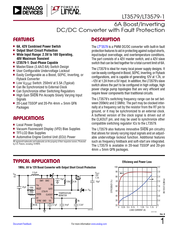
The LT®3579 is a PWM DC/DC converter with built-in fault protection Features to aid in protecting against output shorts, input/output overvoltage, and overtemperature conditions. The part consists of a 42V master switch, and a 42V slave switch that can be tied together for a total current limit of 6A. The LT3579 is ideal for many local power supply designs. It can be easily configured in Boost, SEPIC, Inverting, or Flyback configurations, and is capable of generating 12V at 1.7A, or
- 12V at 1.2A from a 5V input. In addition, the LT3579’s slave switch allows the part to be configured in high voltage, high power charge pump topologies that are very efficient and require fewer ponents than traditional circuits. The LT3579’s switching frequency range can be set bet ween 200k Hz and 2.5MHz. The part may be clocked internally at a frequency set by the resistor from the RT pin to ground, or it may be synchronized to an external clock. A buffered version of the clock signal is driven out of the CLKOUT pin, and may be used to...