LTC1693
LTC1693 is High Speed Single/Dual MOSFET Drivers manufactured by Linear Technology.
LTC1693 High Speed Single/Dual MOSFET Drivers
Features s s
DESCRIPTIO s s s s s s s
Dual MOSFET Drivers in SO-8 Package or Single MOSFET Driver in MSOP Package 1GΩ Electrical Isolation Between the Dual Drivers Permits High/Low Side Gate Drive 1.5A Peak Output Current 16ns Rise/Fall Times at VCC = 12V, CL = 1n F Wide VCC Range: 4.5V to 13.2V CMOS patible Inputs with Hysteresis, Input Thresholds are Independent of VCC Driver Input Can Be Driven Above VCC Undervoltage Lockout Thermal Shutdown
The LTC®1693 family drives power MOSFETs at high speed. The 1.5A peak output current reduces switching losses in MOSFETs with high gate capacitance. The LTC1693-1 contains two noninverting drivers. The LTC1693-2 contains one noninverting and one inverting driver. The LTC1693-1 and LTC1693-2 drivers are electrically isolated and independent. The LTC1693-3 is a single driver with an output polarity select pin. The LTC1693 has VCC independent CMOS input thresholds with 1.2V of typical hysteresis. The LTC1693 can level-shift the input logic signal up or down to the rail-torail VCC drive for the external MOSFET. The LTC1693 contains an undervoltage lockout circuit and a thermal shutdown circuit. Both circuits disable the external N-channel MOSFET gate drive when activated. The LTC1693-1 and LTC1693-2 e in an 8-lead SO package. The LTC1693-3 es in an 8-lead MSOP package.
, LTC and LT are registered trademarks of Linear Technology Corporation.
U APPLICATIO S s s s s s
Power Supplies High/Low Side Drivers Motor/Relay Control Line Drivers Charge Pumps
TYPICAL APPLICATIO
VIN 48VDC ±10% RETURN
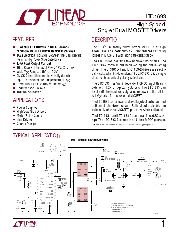
Two Transistor Foward Converter
+
C1 330µF 63V C2 1.5µF 63V
R1 0.068Ω Q1 MTD20NO6HD
12V C5 1µF 17 C11 0.1µF C9 1800p F 5% NPO R5 2.49k 1% 1 2 4 3 5 6 7 10 C10 0.1µF C14 3300p F R9 12k C12 100p F 12VIN BOOST LT1339 SYNC 5VREF SL/ADJ CT IAVG SS VC VREF SGND C15 0.1µF 8 TS SENSE + SENSE
- BG PHASE RUN/SHDN VFB PGND 15 18 11 TG 20 19 BAT54 R6 100Ω LTC1693CS8-2 1 8 VCC1 IN1 2 7 GND1 OUT1...