LTC5505-2
LTC5505-2 is (LTC5505-1/-2) RF Power Detector manufactured by Linear Technology.
- Part of the LTC5505-1 comparator family.
- Part of the LTC5505-1 comparator family.
..
LTC5505-1/LTC5505-2 RF Power Detector with Buffered Output and >40d B Dynamic Range
Features s
DESCRIPTIO s s s s s s s
Internal Schottky Diode RF Detector with Two Input Power Ranges: LTC5505-1,
- 28d Bm to 18d Bm LTC5505-2,
- 32d Bm to 12d Bm Wide Input Frequency Range: 300MHz to 3GHz (LTC5505-1); 300MHz to 3.5GHz (LTC5505-2) Temperature pensated Buffered Detector Output Wide VCC Range of 2.7V to 6V Low Operating Current: 0.5m A Low Shutdown Current: <2µA Low Profile (1mm) Thin SOTTM Package
The LTC®5505-X is an RF power detector for RF applications operating in the 300MHz to 3.5GHz range. A temperature pensated Schottky diode peak detector and buffer amplifier are bined in a small 5-pin Thin SOT package. The supply voltage range is optimized for operation from a single lithium-ion cell or 3x Ni MH. The RF input voltage is peak detected using an on-chip Schottky diode. The detected voltage is buffered and supplied to the VOUT pin. A power saving shutdown mode reduces supply current to less than 2µA. The LTC5505-1 operates with input power levels from
- 28d Bm to 18d Bm. The LTC5505-2 operates with input power levels from
- 32d Bm to 12d Bm.
, LTC and LT are registered trademarks of Linear Technology Corporation. Thin SOT is a trademark of Linear Technology Corporation
U APPLICATIO S s s s s s s
Multimode Mobile Phone Products PCS Devices Wireless Data Modems Wireless and Cable Infrastructure RF Power Alarm Envelope Detector
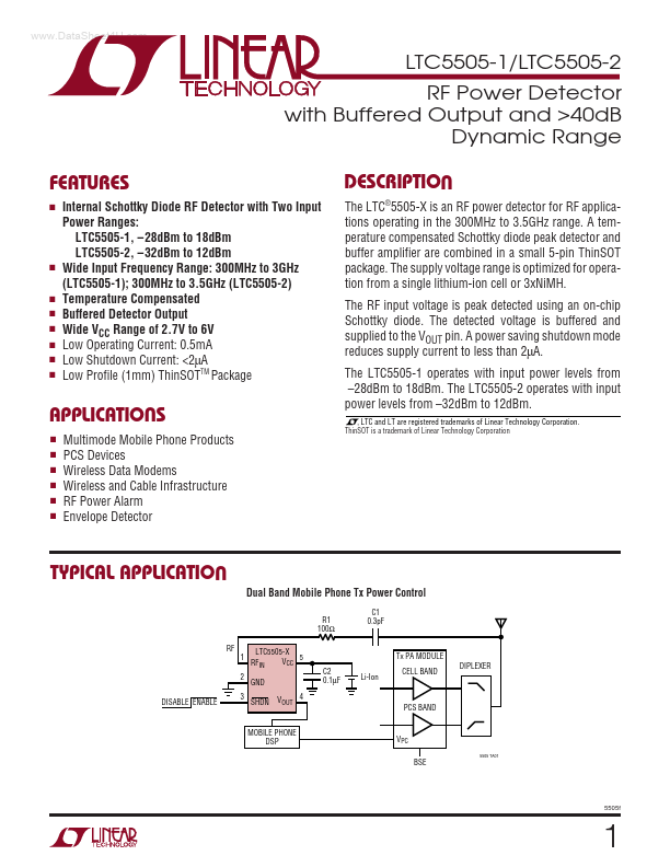
TYPICAL APPLICATIO
Dual Band Mobile Phone Tx Power Control
R1 100Ω RF 1 2 DISABLE ENABLE 3 LTC5505-X VCC 5 RFIN GND SHDN VOUT 4 C1 0.3p F
Tx PA MODULE C2 0.1µF Li-Ion CELL BAND DIPLEXER
PCS BAND
MOBILE PHONE DSP
5505 TA01
5505f
LTC5505-1/LTC5505-2
ABSOLUTE
(Note 1)
AXI U RATI GS
U W U PACKAGE/ORDER I FOR ATIO
ORDER PART NUMBER
TOP VIEW RFIN 1 GND 2 SHDN 3 4 VOUT 5 VCC
VCC, VOUT to GND ....................................
- 0.3V to 6.5V RF Voltage LTC5505-1 ......................................