LTC6416
LTC6416 is 2 GHz Low Noise Differential 16-Bit ADC Buffer manufactured by Linear Technology.
..
Features n n n n n n n n n n n n n n
LTC6416 2 GHz Low Noise Differential 16-Bit ADC Buffer DESCRIPTION
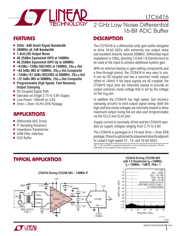
The LTC®6416 is a differential unity gain buffer designed to drive 16-bit ADCs with extremely low output noise and excellent linearity beyond 300MHz. Differential input impedance is 12kΩ, allowing 1:4 and 1:8 transformers to be used at the input to achieve additional system gain. With no external biasing or gain setting ponents and a flow-through pinout, the LTC6416 is very easy to use. It can be DC-coupled and has a mon mode output offset of
- 40m V. If the input signals are AC-coupled, the LTC6416 input pins are internally biased to provide an output mon mode voltage that is set by the voltage on the VCM pin. In addition the LTC6416 has high speed, fast recovery clamping circuitry to limit output signal swing. Both the high and low clamp voltages are internally biased to allow maximum output swing but are also user programmable via the CLLO and CLHI pins. Supply current is nominally 42m A and the LTC6416 operates on supply voltages ranging from 2.7V to 3.9V. The LTC6416 is packaged in a 10-lead 3mm × 2mm DFN package. Pinout is optimized for placement directly adjacent to Linear’s high speed 12-, 14- and 16-bit ADCs.
L, LT, LTC and LTM are registered trademarks of Linear Technology Corporation. All other trademarks are the property of their respective owners.
2GHz
- 3d B Small Signal Bandwidth 300MHz ±0.1d B Bandwidth 1.8n V/√Hz Output Noise 46.25d Bm Equivalent OIP3 at 140MHz 40.25d Bm Equivalent OIP3 Up to 300MHz
- 81d Bc/- 72d Bc HD2/HD3 at 140MHz, 2VP-P Out
- 84.5d Bc IM3 at 140MHz, 2VP-P Out posite
- 74d Bc/- 67.5d Bc HD2/HD3 at 300MHz, 2VP-P Out
- 72.5d Bc IM3 at 300MHz, 2VP-P Out posite Programmable High Speed, Fast Recovery Output Clamping DC-Coupled Signal Path Operates on Single 2.7V to 3.9V Supply Low Power: 150m W on 3.6V 2mm × 3mm 10-Pin DFN Package
APPLICATIONS n n n n n
Differential ADC Driver IF Sampling Receivers Impedance...