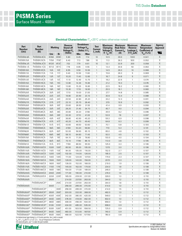
MAXIMUM RATINGS
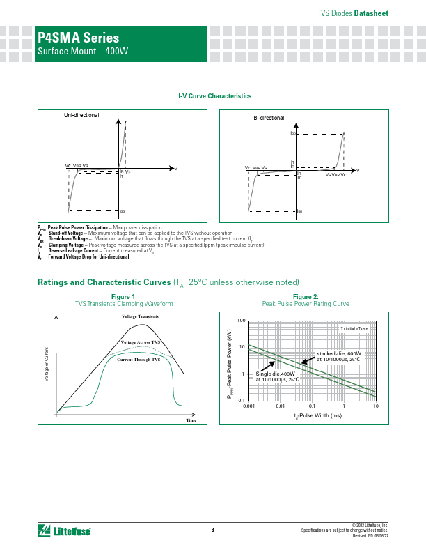
and Thermal Characteristics (TA=25OC unless otherwise noted) Parameter Symbol Value Unit Peak Pulse Power Dissipation at TA=25°C by 10/1000us Waveform(Fig.2)(Note 1), PPPM 400 W (Note 2)Single Die Parts Peak Pulse Power Dissipation at TA=25°C by 10/1000us Waveform(Fig.2)(Note 1), PPPM 600 W (Note 2) Stacked Die Parts(Note 5) Power Dissipation on Infinite Heat Sink at TL=50OC PD 3.3 W Peak Forward Surge Current, 8.3ms Single Half Sine Wave (Note 3) IFSM 60 A Maximum Instantaneous Forward Voltage at 25A for Unidirectional Only (Note 4) VF 3.5/5.0 V Operating Temperature Range Storage Temperature Range Typical Thermal Resistance Junction to Lead TJ -65 to 150 °C TSTG -65 to 175 °C RθJL 30 °C/W Typical Thermal Resistance Junction to Ambient RθJA 120 °C/W Notes: 1. Non-repetitive current pulse, per Fig.4 and derated above TJ (initial) =25ºC per Fig. 3. 2. Mounted on 5.0x5.0mm copper pad to each terminal. 3. Measured on 8.3ms single half sine wave or equivalent square wave for unidirectional device only. Littelfuse