MX1025D
MX1025D is Low Side GaN and MOSFET Driver manufactured by MAXINMICRO.
description
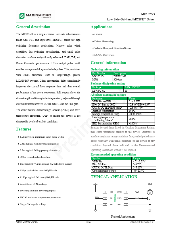
The MX1025D is a single channel low-side enhancementmode Ga N FET and logic-level MOSFET driver for high switching frequency applications. Narrow pulse width capability, fast switching specification, and small pulse distortion bine to significantly enhance Li DAR, To F, and Power Converter performance. 1.25ns output pulse width enables more powerful, eye-safe diode pulses. This, bined with 300ns distortion, leads to longer-range, precise Li DAR/To F systems. 2.9ns propagation delay significantly improves the control loop response time and thus overall performance of the power converters. Split output allows the drive strength and timing to be independently adjusted through external resistors between OUTH, OUTL, and the FET gate. The driver features undervoltage lockout (UVLO) and overtemperature protection (OTP) to ensure the device is not damaged in overload or fault conditions.
Features
- 1.25ns typical minimum input pulse width
- 2.5ns typical rising propagation delay
- 2.7ns typical falling propagation delay
- 300ps typical pulse distortion
- Independent 7A pull-up and 5A pull-down current
- 950ps typical rise time 100p F load)
- 1150ps typical fall time (100p F load)
- 2mm×2mm DFN package
- Inverting and non-inverting inputs
- UVLO and over-temperature protection
- Single 5V supply voltage
MX1025D Low Side Ga N and MOSFET Driver
Applications
- Li DAR
- Driver Monitoring
- Vehicle Occupant Detection Sensor
- DC/DC Converters
General information
Ordering information
Part Number MX1025D MPQ
Description
DFN2- 2-6L 3000pcs
Package dissipation rating
Package
RθJA(℃/W)
DFN2- 2-6L
Absolute maximum ratings
Parameter VDD Pin to GND IN+, IN- Pins to GND OUTH, OUTL Pins to GND Junction temperature Storage temperature, Tstg Leading temperature (soldering,10secs)
Value 0 to 5.75V -0.3 to VDD + 0.3V -0.3 to 5.75V 150℃ -50 to 150℃
260℃
ESD Susceptibility HBM
±2000V
Stresses beyond those listed in Absolute Maximum Ratings may cause permanent damage to...