CD4148WTP
Overview
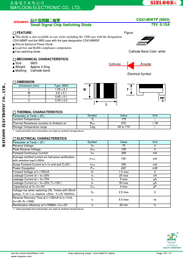
- 55 ± 0.1 W T W 0.8 ± 0.1 T 0.65 ± 0.1 C 0.35 ± 0.2 L C ϭ THERMAL CHARACTERISTICS: Parameter at Tamb = 25к Junction Temperature Thermal Resistance Junction to Ambient air Storage Temperature range
- Valid provided that electrodes are kept at ambient temperature. Symbol Tj RșJA Tstg Value 175 375¹ -65 to 175¹ Unit к к/W к ϭ ELECTRICAL CHARACTERISTICS Parameter at Tamb = 25к Reverse Voltage: Peak Reverse Voltage: Forward Continuous Current: Average rectified current sin half wave rectification with resistive load f>50Hz Surge Forward Current at t<1s and and Tj=25к Power Dissipation Forward Voltage at IF=100mA Leakage Current at = VR=20V Leakage Current at = VR=75V Leakage Current at = VR=20V, TJ=150к Capacitance at VF=VR=0V Voltage rise when switching ON, Testes with 50mA pulses, TP=0.1us, risetime <20ns, Fp=(5-100)KHz. Reverse Recovery Time at IF=100mA to IR=1mA, VR=V6, RL=100ȍ Rectification efficiency at f=100MHZ, VRF=2V
- Valid provided that electrodes are kept at ambient temperature. Symbol VR VRM IFM IF(AV) IFSM Ptot VF IR IR IR Ctot Vfr trr nr Value 75 100 300 150¹ 500 400¹ 1.0 max 25 max 5 max 50 max 4 max
- 5 max
- 0 max 45 min Unit V V mA mA mA mW V nA ȝA ȝA pF V ns % Ref 20100325Rev1105 Chip Switching Diode CD4148WTP (0603) Page: P5 - P1 .":-00/