FCX591
Features
- Power dissipation
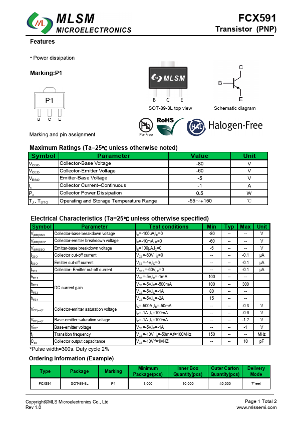
Marking:P1
Transistor (PNP)
P1
B CE
SOT-89-3L top view
Schematic diagram
Marking and pin assignment
Maximum Ratings (Ta=25℃ unless otherwise noted)
Symbol
Parameter
VCBO
Collector-Base Voltage
VCEO
Collector-Emitter Voltage
VEBO
Emitter-Base Voltage
Ic
Collector Current- Continuous
Pc
Collector Power Dissipation
TJ , TSTG
Operating and Storage Temperature Range
Value
-80 -60 -5 -1 0.5 -55~+150
Unit
V V V A W ℃
Electrical Characteristics (Ta=25℃ unless otherwise specified)
Symbol
Parameter
Test conditions
Min
V(BR)CBO Collector-base breakdown voltage
IC=-100μA,IE=0
-80
V(BR)CEO- Collector-emitter breakdown voltage
IC=-10m A,IB=0
-60
V(BR)EBO Emitter-base breakdown...