FMMT495
Features
- Low VCE(sat)
- h FE characterised up to 1A for high current gain hold up
- For general amplification
Transistor (NPN)
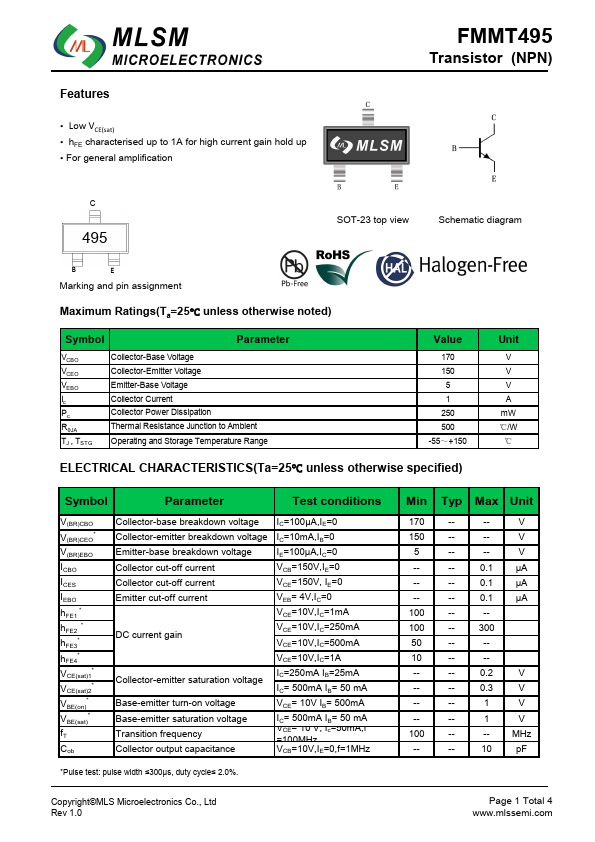
SOT-23 top view
Schematic diagram
Marking and pin assignment
Maximum Ratings(Ta=25℃ unless otherwise noted)
Symbol
Parameter
VCBO VCEO VEBO Ic Pc RθJA TJ , TSTG
Collector-Base Voltage Collector-Emitter Voltage Emitter-Base Voltage Collector Current Collector Power Dissipation Thermal Resistance Junction to Ambient Operating and Storage Temperature Range
Value
170 150
5 1 250 500 -55~+150
ELECTRICAL CHARACTERISTICS(Ta=25℃ unless otherwise specified)
Unit
V V V A m W ℃/W ℃
Symbol
Parameter
Test conditions
V(BR)CBO V(BR)CEO- V(BR)EBO
ICBO
ICES
IEBO h FE1
- h FE2
- h FE3- h FE4- VCE(sat)1- VCE(sat)2- VBE(on)- VBE(sat)- f T
Cob
Collector-base breakdown voltage Collector-emitter breakdown voltage Emitter-base breakdown voltage Collector cut-off current Collector cut-off current Emitter cut-off current
DC current gain
Collector-emitter...