MORESEMI MSC4963W
Dual P-Channel Enhancement Mode Power MOS FET
| Part No. | MSC4963W |
|---|---|
| Datasheet | MSC4963W Download |
| Manufacturer | MORESEMI |
| Description | Dual P-Channel Enhancement Mode Power MOS FET |
| Buy | Stock & Price |
GENERAL FEATURES
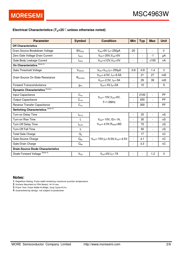
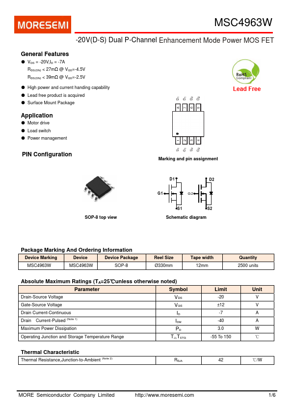
● VDS = -20V,ID = -7A RDS(ON) < 27mΩ @ VGS=-4.5V RDS(ON) < 39mΩ @ VGS=-2.5V● High power and current handing capability
● Lead free product is acquired
● Surface Mount Package Lead Free Application
● Motor drive
● Load switch
● Power management PIN Configuration Marking and pin assignment SOP-8 top view D1 G1 G2 D2 S1 S2 Schematic diagram Package Marking And Ordering Information Device Marking Device Device Package MSC4963W MSC4963W SOP-8 Reel Size Ø330mm Tape width 12mm Quantity 2500 units
ABSOLUTE MAXIMUM RATINGS
(TA=25℃unless otherwise noted) Parameter Symbol Drain-Source Voltage VDS Gate-Source Voltage VGS Drain Current-Continuous Drain Current-Pulsed (Note 1) ID IDM Maximum Power Dissipation PD Operating Junction and Storage Temperature Range TJ,TSTG Limit -20 ±12 -7 -40 3.0 -55 To 150 Unit V V A A W ℃ Thermal Characteristic Thermal Resista