Datasheet4U Logo Datasheet4U.com

SYS32256LK-15 - 256K x 32 SRAM MODULE

Download the SYS32256LK-15 datasheet PDF. This datasheet also covers the SYS32256LK-12 variant, as both devices belong to the same 256k x 32 sram module family and are provided as variant models within a single manufacturer datasheet.

General Description

The SYS32256 is a plastic 8Mbit Static RAM Module offered in Industry Standard 64 pin ZIP and 64 lead SIMM package, organised as 256K x 32.

The module utilises eight fast 256K x 4 SRAMs housed in SOJ packages, and uses double sided surface mount techniques, to achieve a very high density module.

Key Features

  • Access Times of 12/15/17 ns. 64 Pin ZIP & SIMM pinouts. 5 Volt Supply ± 10%. Power Dissipation : Operating (32bit mode) 9.0 W (maximum). Standby (CMOS) -L 1.3 W (maximum). Completely Static Operation. Equal Access and Cycle Times. All Inputs and Outputs Directly TTL Compatible. On-board Supply Decoupling Capacitors. 72 pin SIMM (SYS32256LKX) available.
  • Pin Definition ZIP PD0 D0 D1 D2 D3 Vcc A7 A8 A9 D4 D5.

📥 Download Datasheet

Note: The manufacturer provides a single datasheet file (SYS32256LK-12_MOSAIC.pdf) that lists specifications for multiple related part numbers.

Datasheet Details

Part number SYS32256LK-15
Manufacturer MOSAIC
File Size 92.23 KB
Description 256K x 32 SRAM MODULE
Datasheet download datasheet SYS32256LK-15 Datasheet

Full PDF Text Transcription (Reference)

The following content is an automatically extracted verbatim text from the original manufacturer datasheet and is provided for reference purposes only.

View original datasheet text
www.DataSheet4U.com 256K x 32 SRAM MODULE SYS32256ZK/LK - 12/15/17 
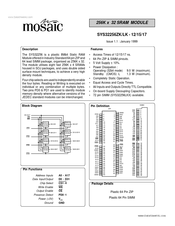
Issue 1.1 : January 1999 Description The SYS32256 is a plastic 8Mbit Static RAM Module offered in Industry Standard 64 pin ZIP and 64 lead SIMM package, organised as 256K x 32. The module utilises eight fast 256K x 4 SRAMs housed in SOJ packages, and uses double sided surface mount techniques, to achieve a very high density module. Four chip selects are used to independently enable the four bytes. Reading or Writing is executed on individual or any combination of multiple bytes. Two pins PD0 & PD1 are used to identify module memory density where alternative versions of the JEDEC standard modules can be interchanged. Block Diagram A0-A17 OE WE 256Kx4 SRAM Features • • • • Access Times of 12/15/17 ns.