Datasheet Details
| Part number | MT4100 |
|---|---|
| Manufacturer | MT Semiconductor |
| File Size | 1.01 MB |
| Description | Dual N- & P-Channel Power MOSFET |
| Datasheet | MT4100-MTSemiconductor.pdf |
|
|
|
Overview: MT4100 
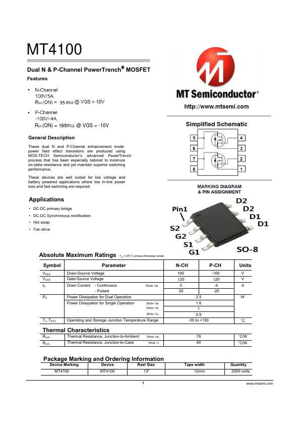
Dual N & P-Channel Po werTrench® MOSFET .
| Part number | MT4100 |
|---|---|
| Manufacturer | MT Semiconductor |
| File Size | 1.01 MB |
| Description | Dual N- & P-Channel Power MOSFET |
| Datasheet | MT4100-MTSemiconductor.pdf |
|
|
|
These dual N and P-Channel enhancement mode power field effect transistors are produced using MOS-TECH Semiconductor’s advanced PowerTrench process that has been especially tailored to minimize on-state ressitance and yet maintain superior switching performance.
These devices are well suited for low voltage and battery powered applications where low in-line power loss and fast switching are required.
$SSOLFDWLRQV '&'&SULPDUEULGJH '&'&6QFKURQRXVUHFWLILFDWLRQ +RWVZDS )DQGULYH Absolute Maximum Ratings TA = 25°C unless otherwise noted Symbol VDSS VGSS ID PD TJ, TSTG Parameter Drain-Source Voltage Gate-Source Voltage Drain Current - Continuous - Pulsed (Note 1a) Power Dissipation for Dual Operation Power Dissipation for Single Operation (Note 1a) (Note 1b) (Note 1c) Operating and Storage Junction Temperature Range Thermal Characteristics RθJA Thermal Resistance, Junction-to-Ambient RθJC Thermal Resistance, Junction-to-Case (Note 1a) (Note 1) N-CH P-CH 100 -100 ±20 ±20 5 -4 20 -20 2.5 1.6 1 0.9 -55 to +150 78 40 Units V V A W °C °C/W °C/W Package Marking and Ordering Information Device Marking Device Reel Size MT4100 MT4100 13" Tape width 12mm Quantity 2500 units ZZZPWVHPLFRP MT4100 Electrical Characteristics Symbol Parameter TA = 25°C unless otherwise noted Test Conditions Off Characteristics BVDSS Drain-Source Breakdown Voltage ΔBVDSS ΔTJ IDSS Breakdown Voltage Temperature Coefficient Zero Gate Voltage Drain Current IGSSF Gate-Body Leakage, Forward IGSSR Gate-Body Leakage, Reverse VGS = 0 V, ID = 250 μA VGS = 0 V, ID = -250 μA ID = 250 μA, Referenced to 25°C ID = -250 µA, Referenced to 25°C VDS = 24 V, VGS = 0 V VDS = -24 V, VGS = 0 V VGS = 20 V, VDS = 0 V VGS = -20 V, VDS = 0 V On Characteristics (Note 2) VGS(th) Gate Threshold Voltage ΔVGS(th) ΔTJ RDS(on) Gat
| Brand Logo | Part Number | Description | Manufacturer |
|---|---|---|---|
![]() |
MT4100 | Broadband CW TWT LAB Amplifier | MCL |
| Part Number | Description |
|---|---|
| MT4110 | 100V 8A N-Channel MOSFET |
| MT4155 | 55V 10A N-Channel Power MOSFET |
| MT4160 | 60V 9A N-Channel Power MOSFET |
| MT4239 | 40V Power MOSFET |
| MT4550 | 40V Power MOSFET |
| MT4600 | Dual N & P-Channel PowerTrench MOSFET |
| MT4605 | 20V Power MOSFET |
| MT4606 | N+P-Channel Enhancement Mode Field Effect Transistor |
| MT4607 | Dual N & P-Channel PowerTrench MOSFET |
| MT4613 | Dual N- & P-Channel Power MOSFET |