MX23J25640
MX23J25640 is 256M-BIT NAND INTERFACE XtraROM manufactured by Macronix.
..
256M-BIT NAND INTERFACE XtraROMTM
Features
- Word organization
- (33,554,432 + 2,097,152Note) by 8 bits
- Page size
- (512 + 16Note) by 8 bits
- Block size
- (16,384 + 512Note) by 8 bits Note : Underlined parts are redundancy and fixed to all FFH.
- Operation mode
- READ mode (1), READ mode (2), READ mode (3), RESET
- Operating supply voltage : VCC = 2.7~3.6V
- Access Time
- Memory cell array to starting address : 7 us (MAX.)
- Read cycle time : 50 ns (MAX.)
- RE access time : 35 ns (MAX.)
- Operating supply current
- During read : 30 mA (MAX.) (50 ns cycle operation)
- During standby (CMOS) : 40 uA (MAX.)
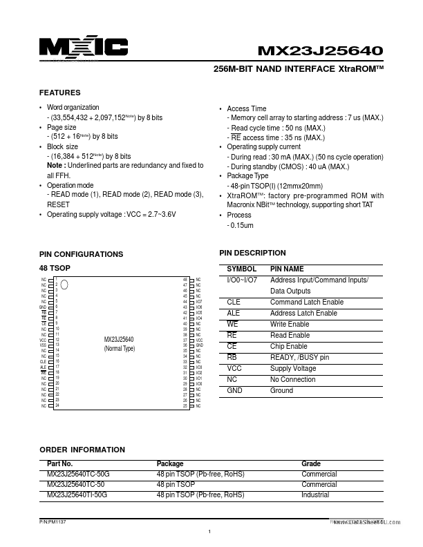
- Package Type
- 48-pin TSOP(I) (12mmx20mm)
-...