Datasheet Summary
..
PRELIMINARY
32M-BIT MASK ROM
Features
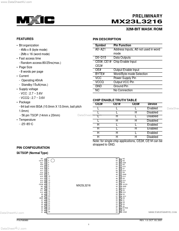
PIN DESCRIPTION
- Bit organization Symbol Pin Function A0~A21 Address Inputs, A0 not used in word
- 4Mb x 8 (byte mode) mode
- 2Mb x 16 (word mode) D0~D15 Data Outputs
- Fast access time CE0#, CE1# Chip Enable Input
- Random access:80/25ns(max.) CE2#
- Page Size OE# Output Enable Input
- 8 words per page BYTE# Word/Byte mode Selection
- Current VCC Power Supply Pin
- Operating:40mA VCCQ Output VCC Pin
- Standby:15uA(max.) GND Ground Pin
- Supply voltage NC No Connection
- VCC : 2.7 ~ 3.6V
- VCCQ : 2.7 ~ 3.6V CHIP ENABLE TRUTH TABLE
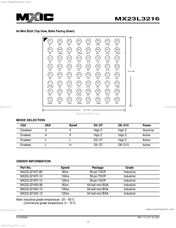
- Package CE2# CE1# CE0# Device
- 64 ball mini BGA (10.0mm X 13.0mm, ball pitch L L L...