MDF7N50TH
MDF7N50TH is N-Channel MOSFET manufactured by MagnaChip.
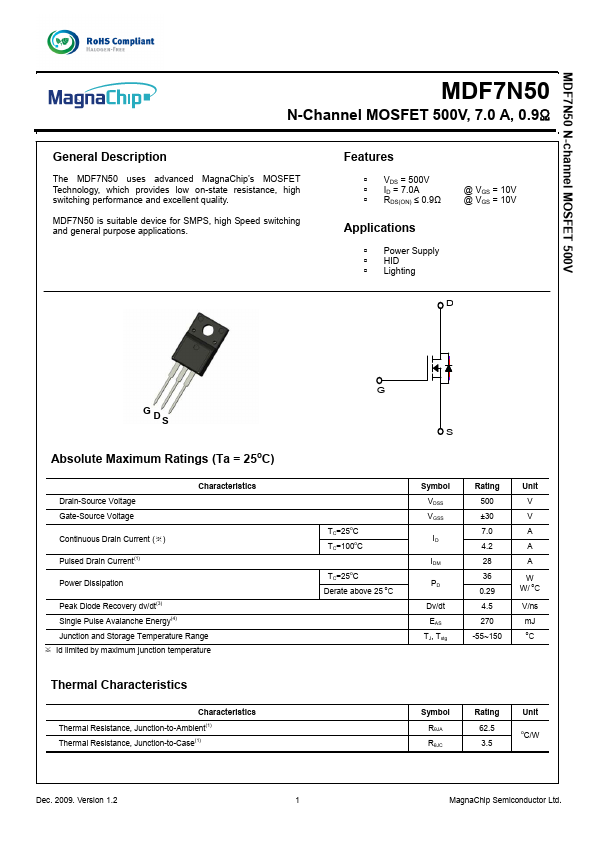
Description
The MDF7N50 uses advanced Magna Chip’s MOSFET Technology, which provides low on-state resistance, high switching performance and excellent quality. MDF7N50 is suitable device for SMPS, high Speed switching and general purpose applications.
Features
VDS = 500V ID = 7.0A RDS(ON) ≤ 0.9Ω @ VGS = 10V @ VGS = 10V
Applications
Power Supply HID Lighting
Absolute Maximum Ratings (Ta = 25o C)
Characteristics Drain-Source Voltage Gate-Source Voltage Continuous Drain Current (※) Pulsed Drain Current Power Dissipation Peak Diode Recovery dv/dt(3) Single Pulse Avalanche Energy
(4) (1)
Symbol VDSS VGSS TC=25 C TC=100 C o o
Rating 500 ±30 7.0 4.2 28 36 0.29 4.5 270 -55~150
Unit V V A A A W W/ o C V/ns m J o
ID IDM
TC=25o C Derate above 25 o C
PD Dv/dt EAS TJ, Tstg
Junction and Storage Temperature Range ※ Id limited by maximum junction temperature
Thermal Characteristics
Characteristics Thermal Resistance, Junction-to-Ambient Thermal Resistance, Junction-to-Case
(1) (1)
Symbol RθJA RθJC
Rating 62.5 3.5
Unit o
C/W
Dec. 2009. Version 1.2
Magna Chip Semiconductor Ltd.
MDF7N50 N-channel MOSFET 500V
Ordering Information
Part Number MDF7N50TH Temp. Range -55~150o C Package TO-220F Packing Tube Ro HS Status Halogen Free
Electrical Characteristics (Ta =25o C)
Characteristics Static Characteristics Drain-Source Breakdown Voltage Gate Threshold Voltage Drain Cut-Off Current Gate Leakage Current Drain-Source ON Resistance Forward Transconductance Dynamic Characteristics Total Gate Charge Gate-Source Charge Gate-Drain Charge Input Capacitance Reverse Transfer Capacitance Output Capacitance Turn-On Delay Time Rise Time Turn-Off Delay Time Fall Time Drain-Source Body Diode Characteristics Maximum Continuous Drain to Source Diode Forward Current Source-Drain Diode Forward Voltage Body Diode Reverse Recovery Time Body Diode Reverse Recovery Charge
Note : 1. Pulse width is based on RθJC & RθJA and the maximum allowed junction temperature of 150°C. 2....