DESCRIPTION
FEATURES
RDS(ON) =150mΩ @ VGS = 10V RDS(ON) =175mΩ @ VGS = 5V APPLICATIONS
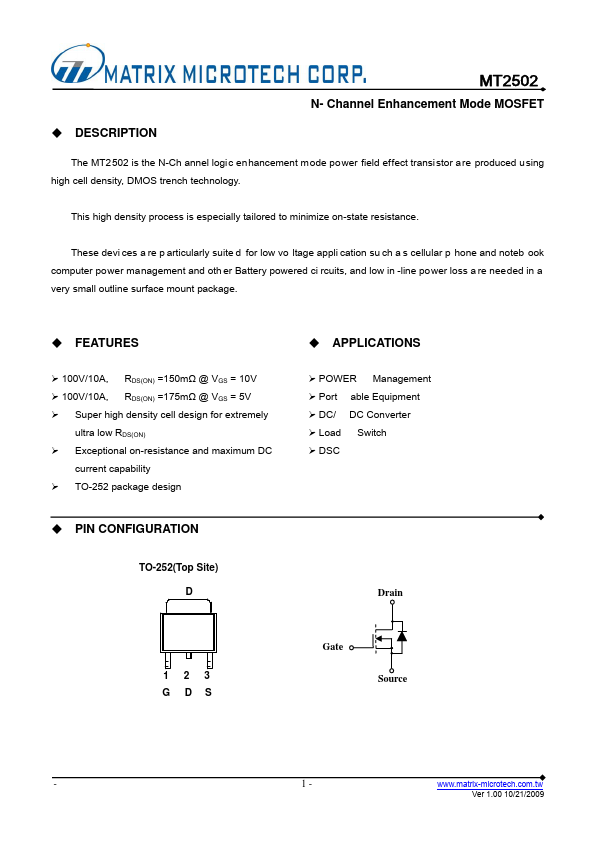
Management ¾ 100V/10A, ¾ 100V/10A, ¾ ¾ ¾ ¾ POWER ¾ Port ¾ DC/ ¾ Load ¾ DSC able Equipment DC Converter Switch Super high density cell design for extremely ultra low RDS(ON) Exceptional on-resistance and maximum DC current capability TO-252 package design PIN CONFIGURATION TO-252(Top Site) D Drain Gate 1 G 2 D 3 S Source - 1- Ver 1.00 10/21/2009 MT2502 N- Channel Enhancement Mode MOSFET ABSOLUTE MAXIMUM RATINGS
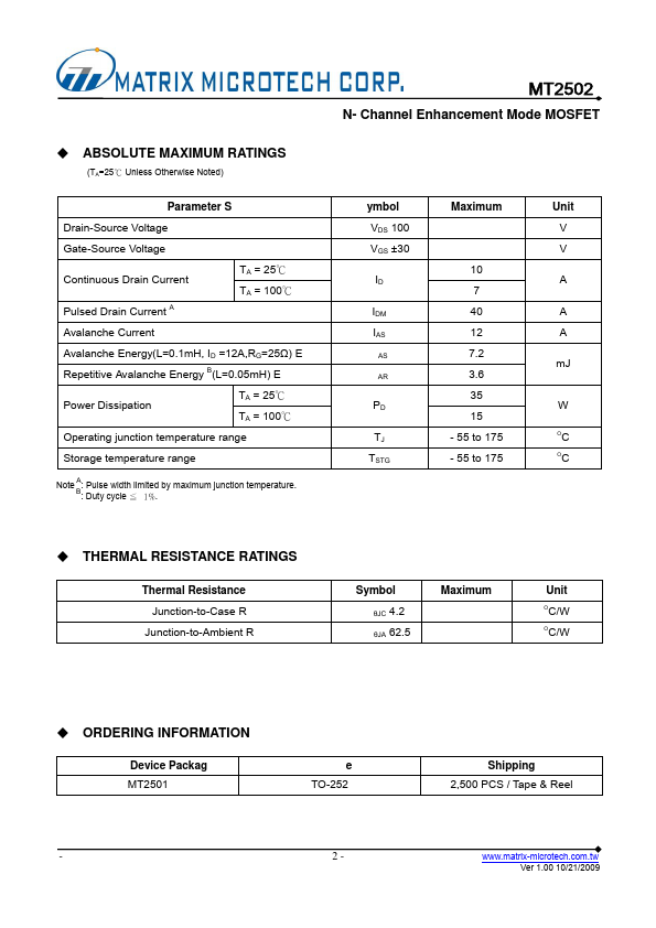
(TA=25℃ Unless Otherwise Noted) Parameter S Drain-Source Voltage Gate-Source Voltage Continuous Drain Current Pulsed Drain Current A Avalanche Current Avalanche Energy(L=0.1mH, ID =12A,RG=25Ω) E Repetitive Avalanche Energy (L=0.05mH) E Power Dissipation TA = 25℃ TA = 100℃ B ymbol VDS 100 VGS ±30 TA = 25℃ TA = 100℃ ID IDM IAS AS AR Maximum Unit V V 10 7 40 12 7.2 3.6 35 15 - 55 to 175 - 55 to 175 A A A mJ PD TJ TSTG W O Operating junction temperature range Storage temperature range Note : Pulse width limited by maximum junction temperature. Matrix Microtech