ME9435A
ME9435A is 30V P-Channel Enhancement Mode MOSFET manufactured by Matsuki.
DESCRIPTION
The ME9435A is the P-Channel logic enhancement mode power field effect transistors, using high cell density, DMOS trench technology. This high density process is especially tailored to minimize on-state resistance. These devices are particularly suited for low voltage application such as cellular phone, notebook puter power management and other battery powered circuits, and lower power loss that are needed in a very small outline surface mount package.
FEATURES
1. 2. -30V/-5.3A, RDS(ON)=40mΩ@VGS=-10V -30V/-4.2A, RDS(ON)=60mΩ@VGS=-4.5V
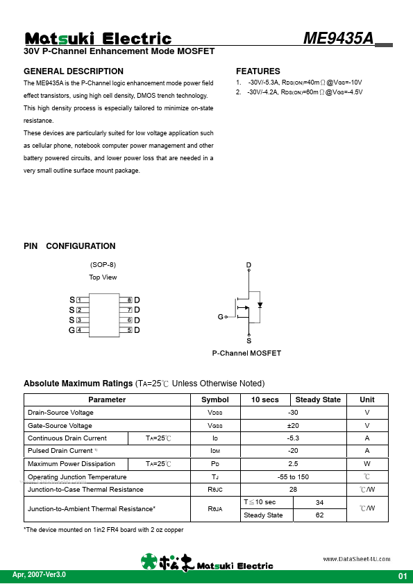
CONFIGURATION
(SOP-8) Top View
Absolute Maximum Ratings (TA=25℃ Unless Otherwise Noted)
Parameter
Drain-Source Voltage Gate-Source Voltage Continuous Drain Current Pulsed Drain Current 1) Maximum Power Dissipation
..
Symbol
VDSS VGSS TA=25℃ ID IDM TA=25℃ PD TJ RθJC RθJA
10 secs
Steady State
-30 ±20 -5.3 -20 2.5
Unit
V V A A W ℃ ℃/W
Operating Junction Temperature Junction-to-Case Thermal Resistance Junction-to-Ambient Thermal Resistance-
-55 to 150 28 T≦10 sec Steady State 34 62
℃/W
- The device mounted on 1in2 FR4 board with 2 oz copper
Apr, 2007-Ver3.0
30V P-Channel Enhancement Mode MOSFET
Electrical Characteristics (TA =25℃ Unless Otherwise Specified)
Symbol
STATIC BVDSS VGS(th) IGSS IDSS RDS(ON) Drain-Source Breakdown Voltage Gate Threshold Voltage Gate Leakage Current Zero Gate Voltage Drain Current Drain-Source On-State Resistance Forward Transconductance VGS=0V, ID=-250μA VDS=VGS, ID=-250μA VDS=0V, VGS=±20V VDS=-24 VGS=0V VGS=-10V, ID= -5.3A VGS=-4.5V, ID= -4.2A 31 40 5 11 -30 -1.0 -2.2 -3.0 ±100 -1 40 60 S V V n A μA mΩ
Parameter
Limit
Min Typ
Max
Unit
DYNAMIC Rg Ciss Coss Crss Qg Qgs Qgd td(on) tr td(off) tf
VDS=-15, ID=-5.3A
Gate resistance Input capacitance Output Capacitance Reverse Transfer Capacitance Total Gate Charge Gate-Source Charge Gate-Drain Charge Turn-On Delay Time Turn-On Rise Time Turn-Off Delay Time Turn-Off Fall Time
VDS=0V, VGS=0V, f=1MHz VDS=-15V, VGS=0V,...