Maxim Integrated AN644
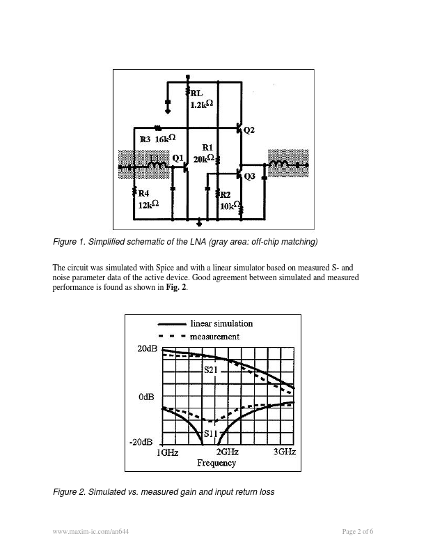
The circuit employs a high-gain common-emitter stage (Q1-RL) and a emitter-follower output stage (Q2-Q3). This approach eliminates the need for coupling capacitors.| Part No. | AN644 |
|---|---|
| Datasheet | AN644 Download |
| Manufacturer |  Maxim Integrated |
| Description | QuickChip Design Example 2 Low Power Silicon BJT LNA for 1.9GHz |
| Buy | Stock & Price |
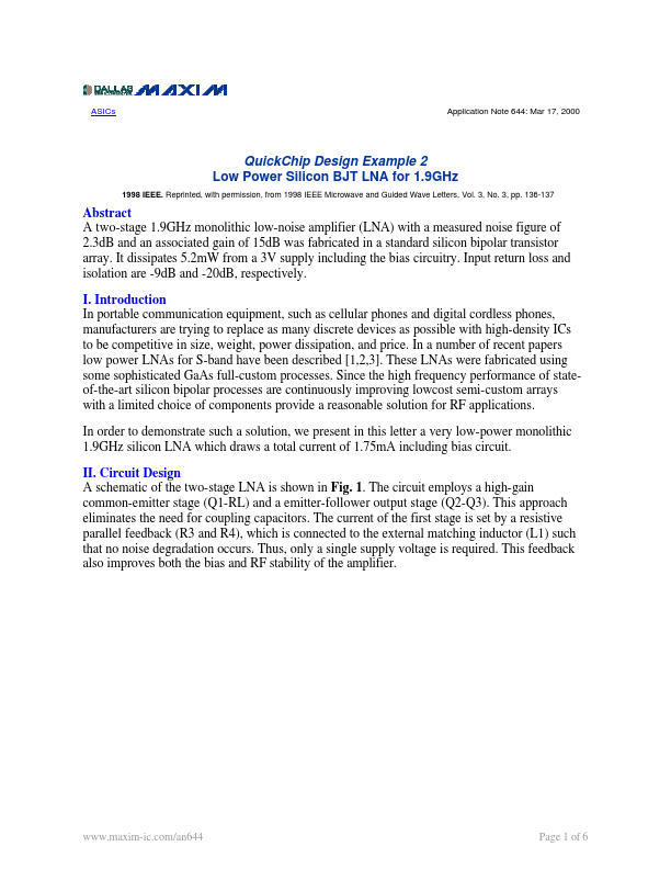
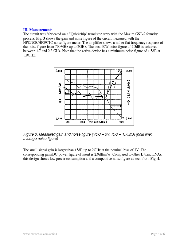
ASICs Application Note 644: Mar 17, 2000 QuickChip Design Example 2 Low Power Silicon BJT LNA for 1.9GHz 1998 IEEE. Reprinted, with permission, from 1998 IEEE Microwave and Guided Wave Letters, Vol. 3, No. 3, pp. 136-137 Abstract A two-stage 1.9GHz monolithic low-noise amplifier (LNA) with a measured noise figure of 2.3dB and an associated gain of 15dB was fabricated in a standard silicon bipolar transistor array. It dissipates 5.2mW from a 3V supply including the bias circuitry. Input return loss and isolation are -9dB and -20dB, respectively. I. Introduction In portable communication equipment, such as cellular phones and digital cordless phones, manufacturers are trying to replace as many discrete devices as possible with high-density ICs to be competitive in size, weight, power dissipation, and price. In a number of recent papers low power LNAs for S-band have been described [1,2,3]. These LNAs were fabricated using some sophisticated GaAs full-custom processes. Since the high freq...