DS1642
DS1642 is Nonvolatile Timekeeping RAM manufactured by Maxim Integrated.
19-5266; Rev 5/10
DS1642 Nonvolatile Timekeeping RAM
.maxim-ic.
Features
- Integrated NV SRAM, Real-Time Clock,
Crystal, Power-Fail Control Circuit, and
Lithium Energy Source
- Standard JEDEC Bytewide 2k x 8 Static
RAM Pinout
- Clock Registers are Accessed Identically to the Static RAM. These Registers are
Resident in the Eight Top RAM Locations
- Totally Nonvolatile with Over 10 Years of
Operation in the Absence of Power
- Access Times of 85ns and 100ns
- Quartz Accuracy ±1 Minute a Month at
+25°C, Factory Calibrated
- BCD-Coded Year, Month, Date, Day, Hours,
Minutes, and Seconds with Leap Year pensation Valid Up to 2100
- Power-Fail Write Protection Allows for
±10% VCC Power Supply Tolerance
- Lithium Energy Source is Electrically
Disconnected to Retain Freshness Until
Power is Applied for the First Time
- UL Recognized
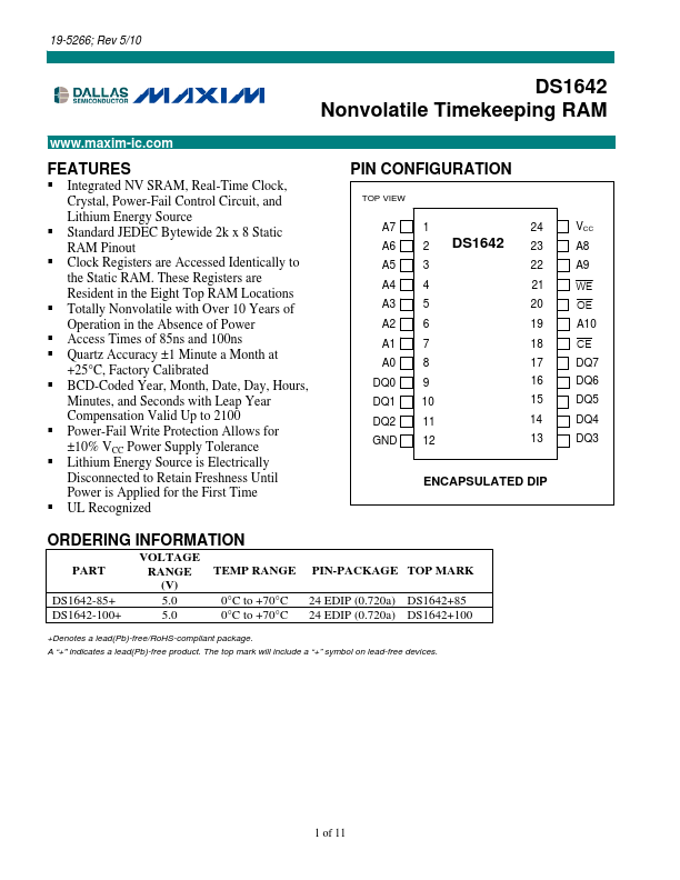
PIN CONFIGURATION
TOP VIEW
A7 A6 A5 A4 A3 A2 A1 A0 DQ0 DQ1 DQ2 GND
2 DS1642
3 4 5
6 7 8 9 10 11...