GENERAL DESCRIPTION
APPLICATIONS
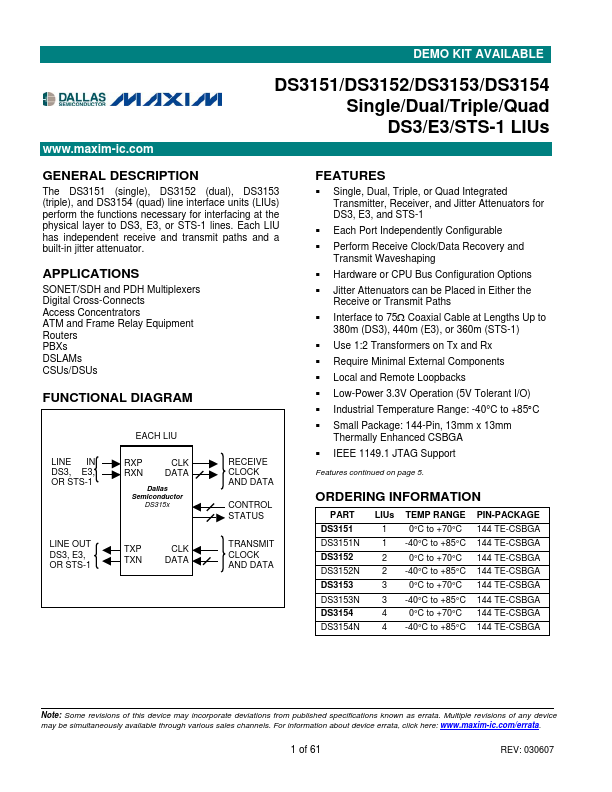
SONET/SDH and PDH Multiplexers Digital Cross-Connects Access Concentrators ATM and Frame Relay Equipment Routers PBXs DSLAMs CSUs/DSUs FUNCTIONAL DIAGRAM LINE IN DS3, E3, OR STS-1 EACH LIU RXP RXN CLK DATA Dallas Semiconductor DS315x LINE OUT DS3, E3, OR STS-1 TXP TXN CLK DATA RECEIVE CLOCK AND DATA CONTROL STATUS TRANSMIT CLOCK AND DATA FEATURES
Single, Dual, Triple, or Quad Integrated Transmitter, Receiver, and Jitter Attenuators for DS3, E3, and STS-1 Each Port Independently Configurable Perform Receive Clock/Data Recovery and Transmit Waveshaping Hardware or CPU Bus Configuration Options Jitter Attenuators can be Placed in Either the Receive or Transmit Paths Interface to 75Ω Coaxial Cable at Lengths Up to 380m (DS3), 440m (E3), or 360m (STS-1) Use 1:2 Transformers on Tx and Rx Require Minimal External Components Local and Remote Loopbacks Low-Power 3.3V Operation (5V Tolerant I/O) Industrial Temperature Range: -40°C to +85°C Small Package: 144-Pin, 13mm x 13mm Thermally Enhanced CSBGA IEEE 1149.1 JTAG Support FEATURES
continued on page 5. Maxim Integrated