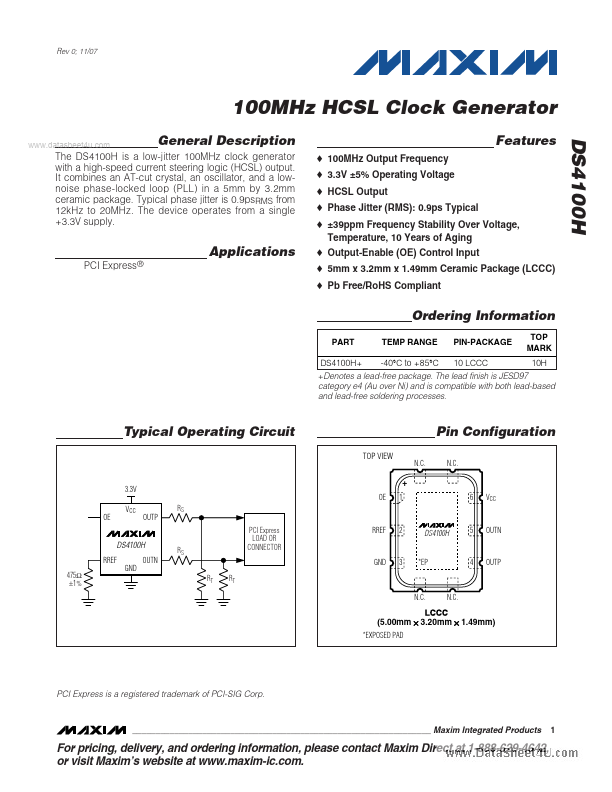
GENERAL DESCRIPTION
♦ 100MHz Output Frequency ♦ 3.3V ±5% Operating Voltage ♦ HCSL Output ♦ Phase Jitter (RMS): 0.9ps Typical FEATURES
DS4100H Typical phase jitter is 0.9psRMS from 12kHz to 20MHz. The device operates from a single +3.3V supply. ♦ ±39ppm Frequency Stability Over Voltage, Temperature, 10 Years of Aging ♦ Output-Enable (OE) Control Input ♦ 5mm x 3.2mm x 1.49mm Ceramic Package (LCCC) ♦ Pb Free/RoHS Compliant APPLICATIONS
PCI Express® Ordering Information PART DS4100H+ TEMP RANGE -40°C to +85°C PIN-PACKAGE 10 LCCC TOP MARK 10H +Denotes a lead-free package. The lead finish is JESD97 category e4 (Au over Ni) and is compatible with both lead-based and lead-free soldering processes. Typical Operating Circuit TOP VIEW + OE VCC OE OUTP PCI Express LOAD OR CONNECTOR RREF 2 RS 1 N.C. Pin Configuration N.C. 3.3V 6 VCC DS4100H 5 OUTN DS4100H RREF 475Ω ±1% GND OUTN RS GND RT RT 3 *EP 4 OUTP N.C. N.C. (5.00mm × 3.20mm × 1.49mm) *EXPOSED PAD PCI Express is a registered trademark of PCI-S... Maxim Integrated