GENERAL DESCRIPTION
FEATURES
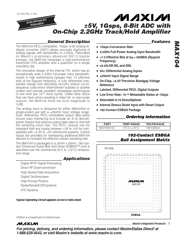
o 1Gsps Conversion Rate o 2.2GHz Full-Power Analog Input Bandwidth o >7.5 Effective Bits at fIN = 500MHz (Nyquist Frequency) o ±0.25LSB INL and DNL o 50Ω Differential Analog Inputs o ±250mV Input Signal Range o On-Chip, +2.5V Precision Bandgap Voltage Reference o Latched, Differential PECL Digital Outputs o Low Error Rate: 10-16 Metastable States at 1Gsps o Selectable 8:16 Demultiplexer o Internal Demux Reset Input with Reset Output o 192-Contact ESBGA Package MAX104 A fully differential comparator design and decoding circuitry reduce out-ofsequence code errors (thermometer bubbles or sparkle codes) and provide excellent metastable performance of one error per 1016 clock cycles. Unlike other ADCs that can have errors resulting in false full- or zero-scale outputs, the MAX104 limits the error magnitude to 1LSB. The analog input is designed for either differential or single-ended use with a ±250mV input voltage range. Dual, differential, PECL-compatible output data paths ensure easy interfacing and include an 8:16 demultiplexer feature that reduces output data rates to one-half the sampling clock rate. Maxim Integrated