Maxim Integrated MAX109
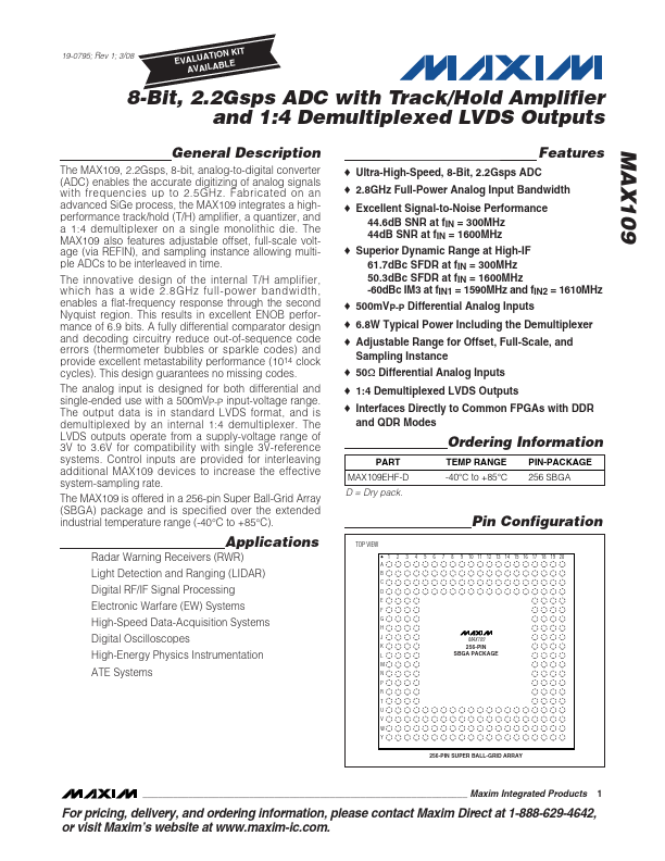
The MAX109, 2.2Gsps, 8-bit, analog-to-digital converter (ADC) enables the accurate digitizing of analog signals with frequencies up to 2.5GHz. The MAX109 also features adjustable offset, full-scale voltage (via REFIN), and sampling instance allowing multiple ADCs to be interleaved in time. The innovative design of the internal T/H amplifier, which has a wide 2.8GHz full-power bandwidth, enables a flat-frequency response through the second Nyquist region.
| Part No. |
MAX109 |
| Datasheet |
MAX109
Download
|
| Manufacturer |
 Maxim Integrated |
| Description |
2.2Gsps ADC |
| Buy |
Stock & Price
|
GENERAL DESCRIPTION
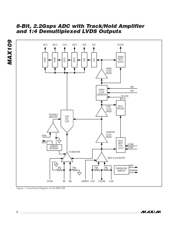
Fabricated on an advanced SiGe process, the MAX109 integrates a highperformance track/hold (T/H) amplifier, a quantizer, and a 1:4 demultiplexer on a single monolithic die. This results in excellent ENOB performance of 6.9 bits. A fully differential comparator design and decoding circuitry reduce out-of-sequence code errors (thermometer bubbles or sparkle codes) and provide excellent metastability performance (1014 clock cycles). This design guarantees no missing codes. The analog input is designed for both differential and single-ended use with a 500mVP-P input-voltage range. The output data is in standard LVDS format, and is demultiplexed by an internal 1:4 demultiplexer. The LVDS outputs operate from a supply-voltage range of 3V to 3.6V for compatibility with single 3V-reference systems. Control inputs are provided for interleaving additional MAX109 devices to increase the effective system-sampling rate. The MAX109 is offered in a 256-pin Super Ball-Grid Array (SBGA) package and is specified over the extended industrial temperature range (-40°C to +85°C).