APPLICATIONS
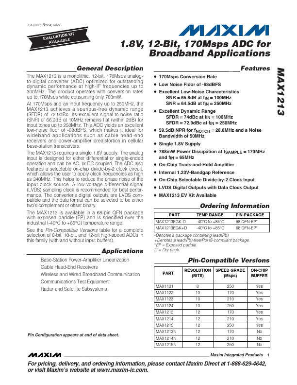
GENERAL DESCRIPTION
FEATURES
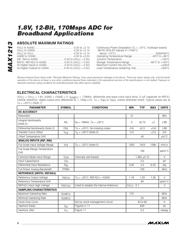
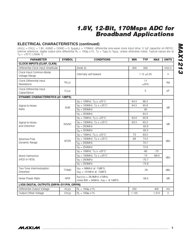
o 170Msps Conversion Rate o Low Noise Floor of -68dBFS o Excellent Low-Noise Characteristics SNR = 65.8dB at fIN = 65MHz SNR = 64.5dB at fIN = 250MHz o Excellent Dynamic Range SFDR = 76.5dBc at fIN = 65MHz SFDR = 72.9dBc at fIN = 250MHz o 59.5dB NPR for fNOTCH = 28.8MHz and a Noise Bandwidth of 50MHz o Single 1.8V Supply o 788mW Power Dissipation at fSAMPLE = 170MHz and fIN = 65MHz o On-Chip Track-and-Hold Amplifier o Internal 1.23V-Bandgap Reference o On-Chip Selectable Divide-by-2 Clock Input o LVDS Digital Outputs with Data Clock Output o MAX1213 EV Kit Available MAX1213 At 170Msps and an input frequency up to 250MHz, the MAX1213 achieves a spurious-free dynamic range (SFDR) of 72.9dBc. This ADC yields an excellent low-noise floor of -68dBFS, which makes it ideal for wideband applications such as cable head-end receivers and power-amplifier predistortion in cellular base-station transceivers. The MAX1213 requires a single 1.8V supply. The analog input is designed for either differential or single-ended operation and can be AC- or DC-coupled. Maxim Integrated