GENERAL DESCRIPTION
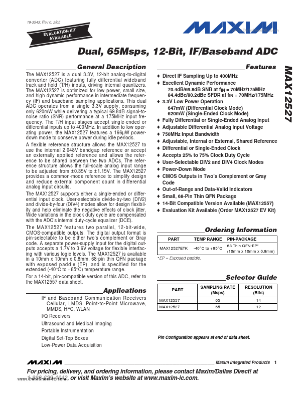
The T/H input stages accept single-ended or differential inputs up to 400MHz. In addition to low operating power, the MAX12527 features a 166µW powerdown mode to conserve power during idle periods. A flexible reference structure allows the MAX12527 to use the internal 2.048V bandgap reference or accept an externally applied reference and allows the reference to be shared between the two ADCs. The reference structure allows the full-scale analog input range to be adjusted from ±0.35V to ±1.15V. The MAX12527 provides a common-mode reference to simplify design and reduce external component count in differential analog input circuits. The MAX12527 supports either a single-ended or differential input clock. User-selectable divide-by-two (DIV2) and divide-by-four (DIV4) modes allow for design flexibility and help eliminate the negative effects of clock jitter. Wide variations in the clock duty cycle are compensated with the ADC’s internal duty-cycle equalizer (DCE). The MAX12527 features two parallel, 12-bit-wide, CMOS-compatible outputs. Maxim Integrated