GENERAL DESCRIPTION
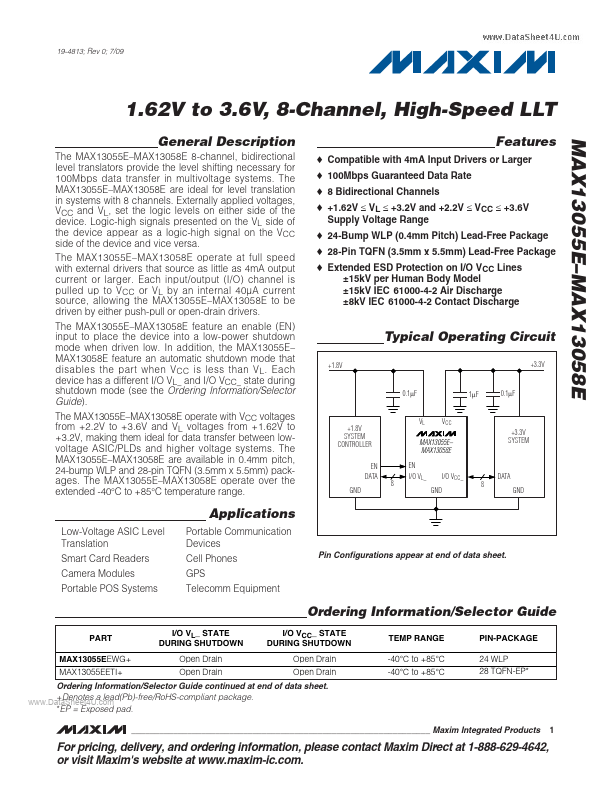
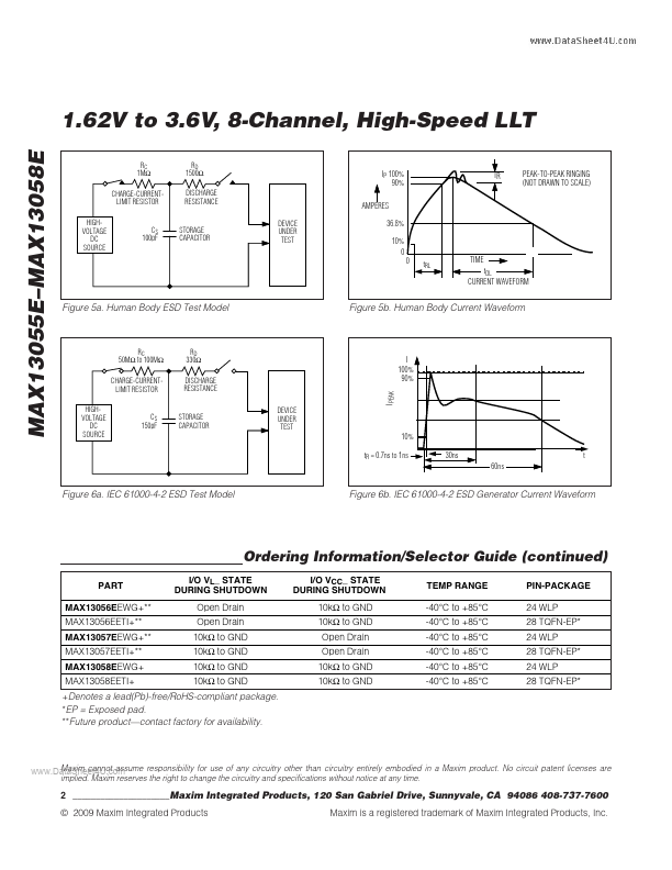
Externally applied voltages, VCC and VL, set the logic levels on either side of the device. Logic-high signals presented on the VL side of the device appear as a logic-high signal on the VCC side of the device and vice versa. Each input/output (I/O) channel is pulled up to VCC or VL by an internal 40µA current source, allowing the MAX13055E–MAX13058E to be driven by either push-pull or open-drain drivers. The MAX13055E–MAX13058E feature an enable (EN) input to place the device into a low-power shutdown mode when driven low. In addition, the MAX13055E– MAX13058E feature an automatic shutdown mode that disables the part when V CC is less than V L . Each device has a different I/O VL_ and I/O VCC_ state during shutdown mode (see the Ordering Information/Selector Guide). The MAX13055E–MAX13058E operate with VCC voltages from +2.2V to +3.6V and VL voltages from +1.62V to +3.2V, making them ideal for data transfer between lowvoltage ASIC/PLDs and higher voltage systems. The MAX13055E–MAX13058E are available in 0.4mm pitch, 24-bump WLP and 28-pin TQFN (3.5mm x 5.5mm) packages. Maxim Integrated