Maxim Integrated MAX14566BE
The MAX14566BE features an additional digital input (CB1) to allow forced charger mode. These devices have enhanced, high electrostatic discharge (ESD) protection on the DP and DM inputs up to Q15kV Human Body Model (HBM).| Part No. | MAX14566BE |
|---|---|
| Datasheet | MAX14566BE Download |
| Manufacturer |  Maxim Integrated |
| Description | USB Host Charger Identification Analog Switches |
| Buy | Stock & Price |

FEATURES
S Hi-Speed USB Switching S Low 4.0pF (typ) On-Capacitance S Low 4.0I (typ) On-Resistance S Ultra-Low 0.1I (typ) On-Resistance Flatness S +2.8V to +5.5V Supply Range S Ultra-Low 3µA (typ) Supply Current S Automatic Current-Limit Switch Control S Automatic USB Charger Identification Circuit S ±15kV High ESD HBM Protection On DP/DM S 2mm x 2mm, 8-Pin TDFN Package S -40NC to +85NC Operating Temperature RangeGENERAL DESCRIPTION
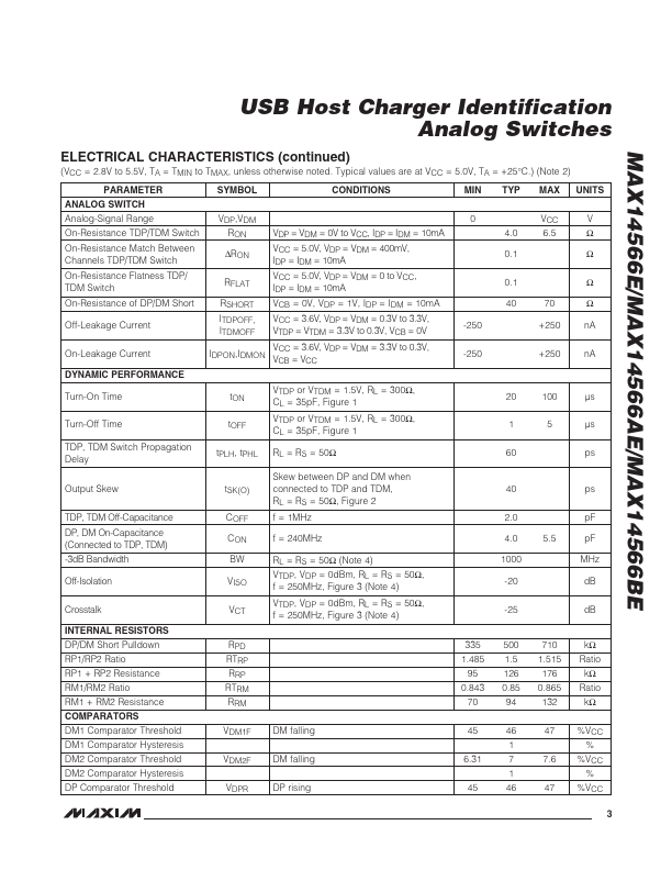
The MAX14566E/MAX14566AE/MAX14566BE are second-generation USB devices that combine Hi-Speed USB analog switches with a USB host charger (dedicated charger) identification circuit. These devices support both the latest USB Battery Charging Specification Revision 1.2 including data contact detection and a set resistor bias for Apple-compliant devices as well as legacy USB D+/Dshort detection using data line pullup. The MAX14566E has a pMOSFET open-drain control output (CEN) and the MAX14566AE has an nMOSFET open-drain control output (CEN) to restart the peripheral connected to the USB host.