MAX4560
MAX4560 is 15kV ESD-Protected / Low-Voltage / CMOS Analog Multiplexers/Switches manufactured by Maxim Integrated.
- Part of the MAX4559 comparator family.
- Part of the MAX4559 comparator family.
Description
The MAX4558/MAX4559/MAX4560 are low-voltage, CMOS analog ICs configured as an 8-to-1 multiplexer (MAX4558), a dual 4-to-1 multiplexer (MAX4559), and a triple single-pole/double-throw (SPDT) switch (MAX4560). Each switch is protected against ±15k V electrostatic discharge (ESD) shocks, without latchup or damage. These CMOS devices can operate continuously from dual supplies of ±2V to ±6V or from a +2V to +12V single supply. Each switch can handle Rail-to-Rail® analog signals. The off-leakage current is only 1n A at +25°C or 10n A at +85°C max. All digital inputs have +0.8V to +2.4V logic thresholds, ensuring TTL/CMOS-logic patibility when using a single +5V supply or dual ±5V supplies.
Applications
Battery-Operated Equipment Audio and Video Signal Routing Low-Voltage Data-Acquisition Systems munications Circuits High-ESD Environments
Rail-to-Rail is a registered trademark of Nippon Motorola, Ltd.
Features o ESD-Protected X, Y, Z and X_, Y_, Z_ Pins ±15k V (Human Body Model) ±12k V (IEC 1000-4-2, Air-Gap Discharge) ±8k V (IEC 1000-4-2, Contact Discharge) o Pin-patible with Industry-Standard 74HC4051/74HC4052/74HC4053 o Guaranteed On-Resistance 220Ω with Single +5V Supply 160Ω with ±5V Supply o RON Match Between Channels: 2Ω (typ) o Guaranteed Low leakage Currents 1n A Off-Leakage (at +25°C) 1n A On-Leakage (at +25°C) o TTL-patible Inputs with +5V/±5V Supplies o Low Distortion: < 0.02% (600Ω) o Low Crosstalk: < -93d B (50Ω) o High Off-Isolation: < -96d B (50Ω)
Ordering Information
PART MAX4558CEE MAX4558CSE MAX4558CPE
TEMP. RANGE 0°C to +70°C 0°C to +70°C 0°C to +70°C
PIN-PACKAGE 16 QSOP 16 Narrow SO 16 Plastic DIP
Ordering Information continued at end of data sheet.
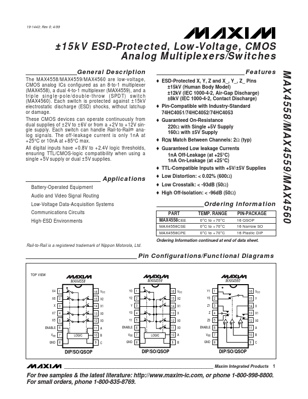
Pin Configurations/Functional Diagrams
TOP VIEW
MAX4558
X4 1 X6 2 X3 X7 4 X5 5 ENABLE 6 VEE 7 GND 8
LOGIC
16 VCC 15 X2 14 X1 13 X0 12 X3 11 A 10 B 9C
DIP/SO/QSOP
MAX4559
Y0 1 Y2 2 Y3 Y3 4 Y1 5 ENABLE 6 VEE 7 GND 8
LOGIC
16 VCC 15 X2 14 X1 13 X 12 X0 11 X3 10 A...