GENERAL DESCRIPTION
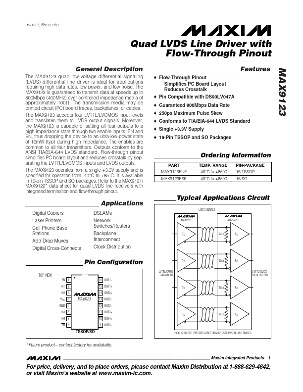
The MAX9123 accepts four LVTTL/LVCMOS input levels and translates them to LVDS output signals. Moreover, the MAX9123 is capable of setting all four outputs to a high-impedance state through two enable inputs, EN and EN, thus dropping the device to an ultra-low-power state of 16mW (typ) during high impedance. The enables are common to all four transmitters. Outputs conform to the ANSI TIA/EIA-644 LVDS standard. Flow-through pinout simplifies PC board layout and reduces crosstalk by separating the LVTTL/LVCMOS inputs and LVDS outputs. The MAX9123 operates from a single +3.3V supply and is specified for operation from -40°C to +85°C. It is available in 16-pin TSSOP and SO packages. Refer to the MAX9121/ MAX9122* data sheet for quad LVDS line receivers with integrated termination and flow-through pinout. Digital Copiers Laser Printers Cell Phone Base Stations Add Drop Muxes Digital Cross-Connects APPLICATIONS
DSLAMs Network Switches/Routers Backplane Interconnect Clock... Maxim Integrated