GENERAL DESCRIPTION
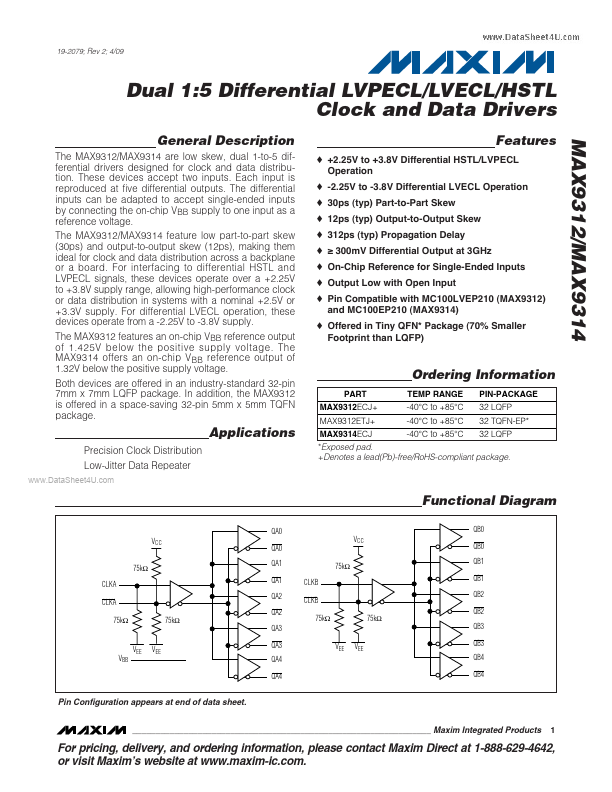
The MAX9312/MAX9314 are low skew, dual 1-to-5 differential drivers designed for clock and data distribution. These devices accept two inputs. Each input is reproduced at five differential outputs. The differential inputs can be adapted to accept single-ended inputs by connecting the on-chip VBB supply to one input as a reference voltage. The MAX9312/MAX9314 feature low part-to-part skew (30ps) and output-to-output skew (12ps), making them ideal for clock and data distribution across a backplane or a board. For interfacing to differential HSTL and LVPECL signals, these devices operate over a +2.25V to +3.8V supply range, allowing high-performance clock or data distribution in systems with a nominal +2.5V or +3.3V supply. For differential LVECL operation, these devices operate from a -2.25V to -3.8V supply. In addition, the MAX9312 is offered in a space-saving 32-pin 5mm x 5mm TQFN package. FEATURES
o +2.25V to +3.8V Differential HSTL/LVPECL Operation o -2.25V to -3.8... Maxim Integrated