MAX686
Description
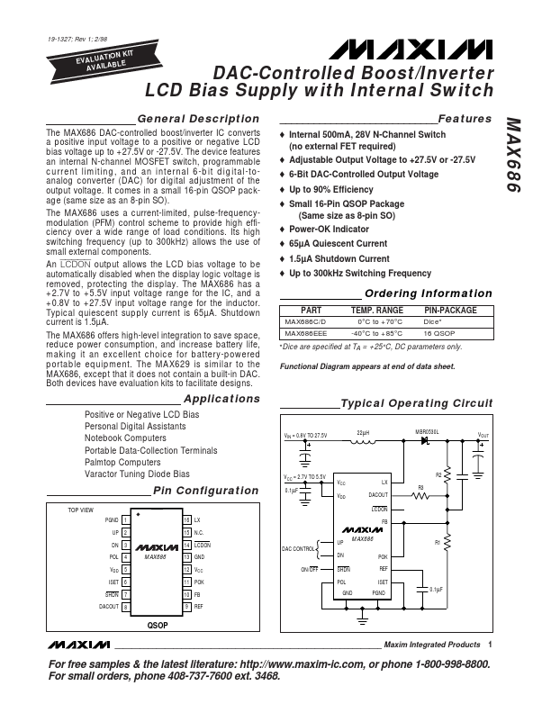
____________________________Features o Internal 500mA, 28V N-Channel Switch (no external FET required) o Adjustable Output Voltage to +27.5V or -27.5V o 6-Bit DAC-Controlled Output Voltage o Up to 90% Efficiency o Small 16-Pin QSOP Package (Same size as 8-pin SO) o Power-OK Indicator o 65µA Quiescent Current o 1.5µA Shutdown Current o Up to 300kHz Switching Frequency MAX686 The MAX686 DAC-controlled boost/inverter IC converts a positive input voltage to a positive or negative LCD bias voltage up to +27.5V or -27.5V.
Key Features
- It es in a small 16-pin QSOP package (same size as an 8-pin SO)
- An LCDON output allows the LCD bias voltage to be automatically disabled when the display logic voltage is removed, protecting the display
- The MAX686 has a +2.7V to +5.5V input voltage range for the IC, and a +0.8V to +27.5V input voltage range for the inductor
- Typical quiescent supply current is 65µA
- Shutdown current is 1.5µA
- The MAX629 is similar to the MAX686, except that it does not contain a built-in DAC
- Both devices have evaluation kits to facilitate designs