MAX9160
MAX9160 is LVDS or LVTTL/LVCMOS Input to 14 LVTTL/LVCMOS Output Clock Driver manufactured by Maxim Integrated.
19-2392; Rev 0; 4/02
LVDS or LVTTL/LVCMOS Input to 14 LVTTL/LVCMOS Output Clock Driver
General Description
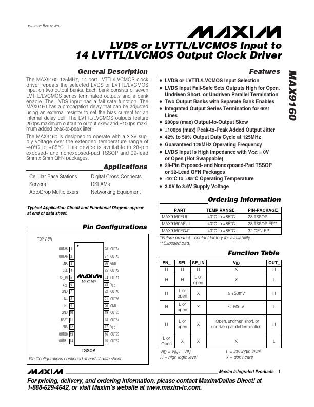
The MAX9160 125MHz, 14-port LVTTL/LVCMOS clock driver repeats the selected LVDS or LVTTL/LVCMOS input on two output banks. Each bank consists of seven LVTTL/LVCMOS series terminated outputs and a bank enable. The LVDS input has a fail-safe function. The MAX9160 has a propagation delay that can be adjusted using an external resistor to set the bias current for an internal delay cell. The LVTTL/LVCMOS outputs feature 200ps maximum output-to-output skew and ±100ps maximum added peak-to-peak jitter. The MAX9160 is designed to operate with a 3.3V supply voltage over the extended...