GENERAL DESCRIPTION
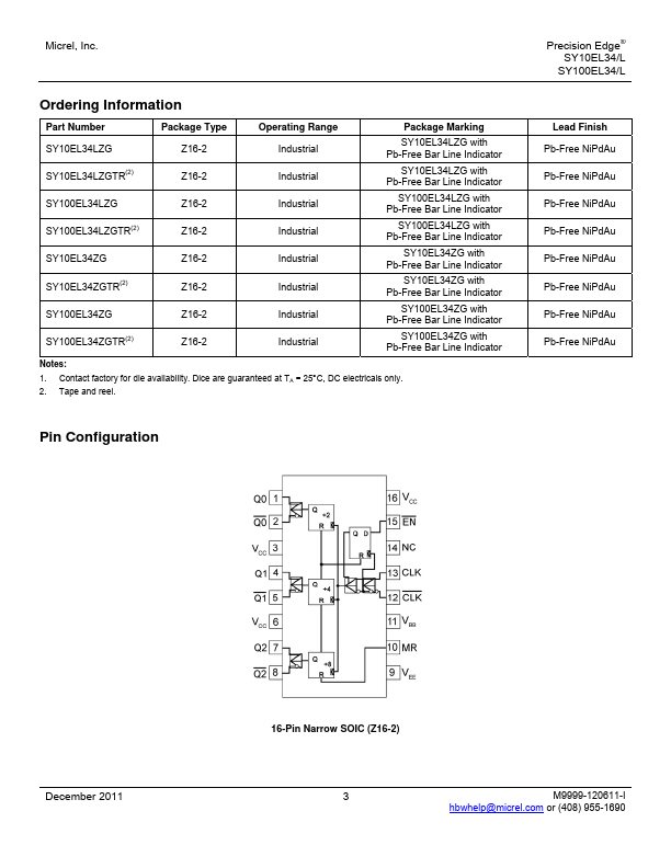
In addition, by using the VBB output, a sinusoidal source can be ACcoupled into the device. If a single-ended input is to be used, the VBB output should be connected to the CLK input and bypassed to ground via a 0.01µF capacitor. The VBB output is designed to act as the switching reference for the input of the EL34/L under single-ended input conditions. As a result, this pin can only source/ sink up to 0.5mA of current. The common enable ( EN ) is synchronous so that the internal dividers will only be enabled/disabled when the internal clock is already in the LOW state. This avoids any chance of generating a runt clock pulse on the internal clock when the device is enabled/disabled as can happen with an asynchronous control. An internal runt pulse could lead to losing synchronization between the internal divider stages. The internal enable flip-flop is clocked on the falling edge of the divider stages. The internal enable flipflop is clocked on the falling edge of the input clock; therefore, all associated specification limits are referenced to the negative edge of the clock input. Micrel