FEATURES
s 725ps max. D to output s Extended 100E VEE range of –4.2V to –5.5V s Differential outputs s Split select architecture s Fully compatible with industry standard 10KH, 100K ECL levels s Internal 75KΩ input pulldown resistors s Fully compatible with Motorola MC10E/100E171 s Available in 28-pin PLCC package DESCRIPTION
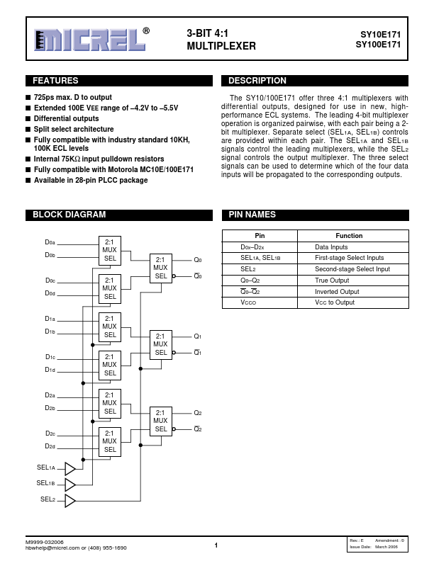
Separate select (SEL1A, SEL1B) controls are provided within each pair. The three select signals can be used to determine which of the four data inputs will be propagated to the corresponding outputs. BLOCK DIAGRAM D0a D0b D0c D0d D1a D1b D1c D1d D2a D2b D2c D2d SEL1A SEL1B SEL2 2:1 MUX SEL 2:1 MUX SEL 2:1 MUX SEL 2:1 MUX SEL 2:1 MUX SEL 2:1 MUX SEL PIN NAMES 2:1 MUX SEL Q0 Q0 Pin D0x–D2x SEL1A, SEL1B SEL2 Q0–Q2 Q0–Q2 VCCO 2:1 MUX SEL Q1 Q1 Function Data Inputs First-stage Select Inputs Second-stage Select Input True Output Inverted Output VCC to Output 2:1 MUX SEL Q2 Q2 M9999-032006 hbwhelp@micrel.com or (408) 955-1690 1 Rev.: E Amendment: /0 Issue Date: March 2006 Micrel, Inc. Micrel