GENERAL DESCRIPTION
The regulator can be disabled via the SHDN pin. While disabled, the output of the regulator is completely isolated from the circuit’s input supply, and the supply current is reduced to less than 5µA to help extend battery life. FEATURES
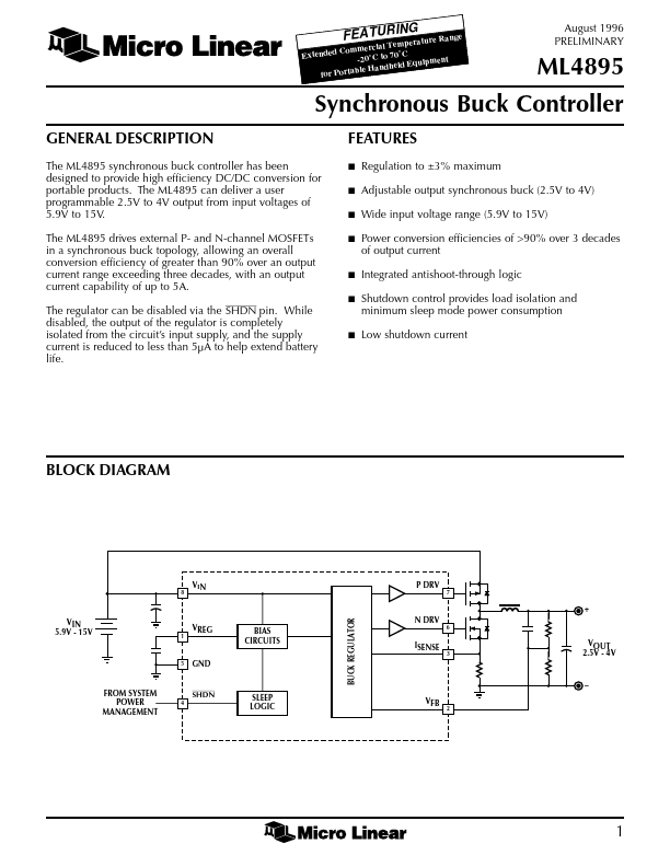
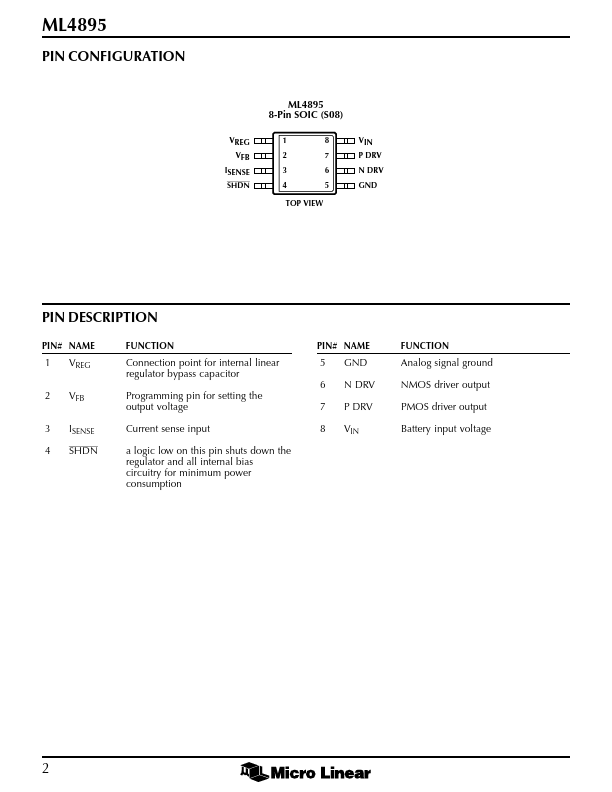
s s s s Regulation to ±3% maximum Adjustable output synchronous buck (2.5V to 4V) Wide input voltage range (5.9V to 15V) Power conversion efficiencies of >90% over 3 decades of output current Integrated antishoot-through logic Shutdown control provides load isolation and minimum sleep mode power consumption Low shutdown current s s s BLOCK DIAGRAM 8 VIN P DRV 7 + VIN 5.9V - 15V 1 VREG BUCK REGULATOR N DRV 6 BIAS CIRCUITS ISENSE 3 VOUT 2.5V - 4V 5 GND – VFB 2 FROM SYSTEM POWER MANAGEMENT SHDN 4 SLEEP LOGIC 1 ML4895 PIN CONFIGURATION ML4895 8-Pin SOIC (S08) VREG VFB ISENSE SHDN 1 2 3 4 TOP VIEW 8 7 6 5 VIN P DRV N DRV GND PIN DESCRIPTION
PIN# NAME FUNCTION PIN# NAME FUNCTION 1 2 3 4 VREG VFB ISENSE SHDN Connection point for internal li... Micro Linear