PL613-01
Overview
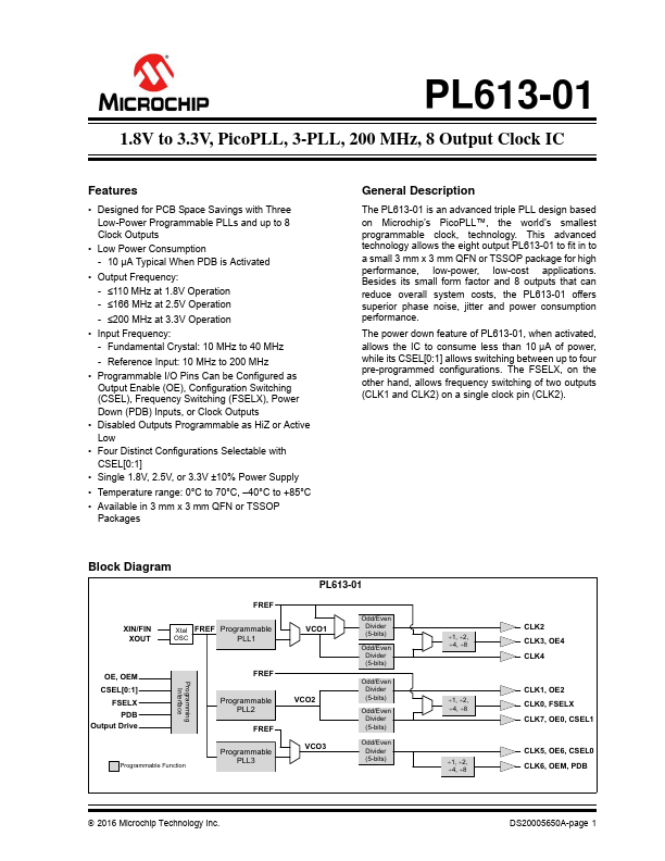
The PL613-01 is an advanced triple PLL design based on Microchip’s PicoPLL™, th.
- Designed for PCB Space Savings with Three Low-Power Programmable PLLs and up to 8 Clock Outputs
- Low Power Consumption - 10 µA Typical When PDB is Activated
- Output Frequency: - ≤110 MHz at 1.8V Operation - ≤166 MHz at 2.5V Operation - ≤200 MHz at 3.3V Operation
- Input Frequency: - Fundamental Crystal: 10 MHz to 40 MHz - Reference Input: 10 MHz to 200 MHz
- Programmable I/O Pins Can be Configured as Output Enable (OE), Configuration Switching (CSEL), Frequency Switching (FSELX), Power Down (PDB) Inputs, or Clock Outputs
- Disabled Outputs Programmable as HiZ or Active Low
- Four Distinct Configurations Selectable with CSEL[0:1]
- Single 1.8V, 2.5V, or 3.3V ±10% Power Supply
- Temperature range: 0°C to 70°C, -40°C to +85°C
- Available in 3 mm x 3 mm QFN or TSSOP Packages