Microchip Technology TC1240A
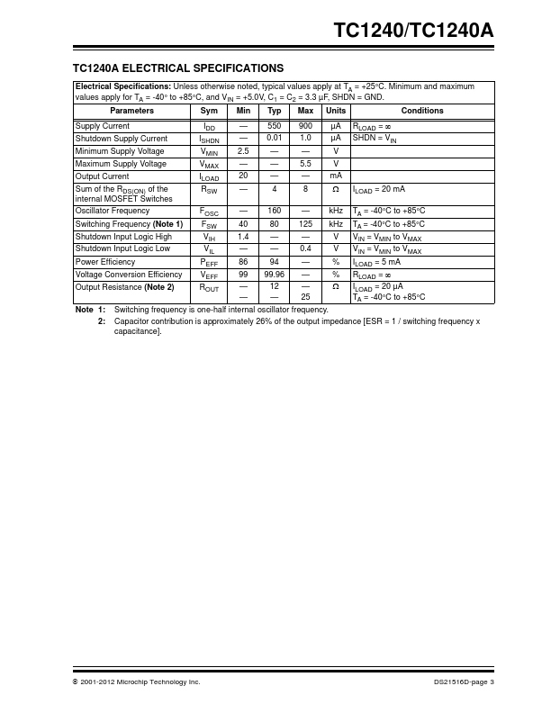
the TC1240A doubles an input voltage that can range from +2.5V to +5.5V. The TC1240 and TC1240A have an active-high shutdown that limits the current consumption of the devices to less than 1 µA.| Part No. | TC1240A |
|---|---|
| Datasheet | TC1240A Download |
| Manufacturer |  Microchip Technology |
| Description | Positive Doubling Charge Pumps |
| Buy | Stock & Price |
FEATURES
●●
●
●
●
●
●
●
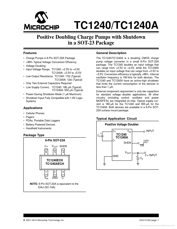
● Charge Pumps in 6-Pin SOT-23A Package >99% Typical Voltage Conversion Efficiency Voltage Doubling Input Voltage Range, TC1240: +2.5V to +4.0V, TC1240A: +2.5V to +5.5V Low Output Resistance, TC1240: 17 (Typical) TC1240A: 12 (Typical) Only Two External Capacitors Required Low Supply Current, TC1240: 180 µA (Typical) TC1240A: 550 µA (Typical) Power-Saving Shutdown Mode (1 µA Maximum) Shutdown Input Fully Compatible with 1.8V Logic Systems
GENERAL DESCRIPTION
The TC1240/TC1240A is a doubling CMOS charge pump voltage converter in a small 6-Pin SOT-23A package. The TC1240 doubles an input voltage that can range from +2.5V to +4.0V, while Conversion efficiency is typically >99%. Internal oscillator frequency is 160 kHz for both devices. External component requirement is only two capacitors for standard voltage doubler applications. All other circuitry (including control, oscillator and power MOSFETs) are integrated on-chip. Typical supply current is 180 µA for the TC1240 and 550 µA for the TC1240A.