Microchip Technology TC1302A
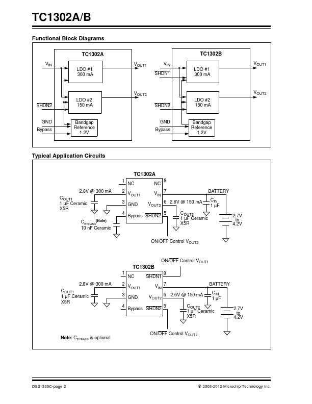
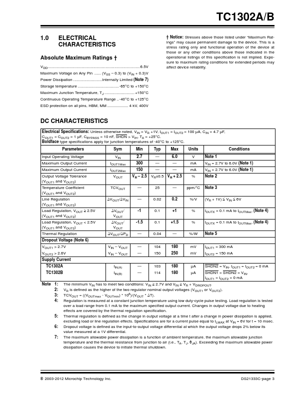
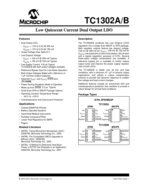
The TC1302A/B combines two Low Dropout (LDO) regulators into a single 8-pin MSOP or DFN package. Both regulator outputs feature low dropout voltage, 104 mV @ 300 mA for VOUT1, 150 mV @ 150 mA for VOUT2, low quiescent current consumption, 58 µA each and a typical regulation accuracy of 0.5%. The TC1302A/B is stable over all line and load conditions, with a minimum of 1 µF of ceramic output capacitance, and utilizes a unique compensation scheme to provide fast dynamic response to sudden line voltage and load current changes.| Part No. | TC1302A |
|---|---|
| Datasheet | TC1302A Download |
| Manufacturer |  Microchip Technology |
| Description | Low Quiescent Current Dual Output LDO |
| Buy | Stock & Price |
FEATURES
● Dual Output LDO: - VOUT1 = 1.5V to 3.3V @ 300 mA - VOUT2 = 1.5V to 3.3V @ 150 mA● Output Voltage (See Table 8-1)
● Low Dropout Voltage: - VOUT1 = 104 mV @ 300 mA Typical - VOUT2 = 150 mV @ 150 mA Typical
● Low Supply Current: 116 µA Typical TC1302A/B with both output voltages available
● Reference Bypass Input for Low-Noise Operation
● Both Output Voltages Stable with a Minimum of 1 µF Ceramic Output Capacitor
● Separate VOUT1 and VOUT2 SHDN pins (TC1302B)
● Power-Saving Shutdown Mode of Operation
● Wake-up from SHDN: 5.3 µs. Typical
● Small 8-pin DFN or MSOP Package Options
● Operating Junction Temperature Range: - -40°C to +125°C
● Overtemperature and Overcurrent Protection
APPLICATIONS
● Cellular/GSM/PHS Phones● Battery-Operated Systems
● Hand-Held Medical Instruments
● Portable Computers/PDAs
● Linear Post-Regulators for SMPS
● Pagers Related Literature
● AN765, “Using Microchip’s Micropower LDOs”, DS00765, Microchip Technology Inc., 2002
● AN766, “Pin-Compatible CMOS...