MT8VDDT3264A
Key Features
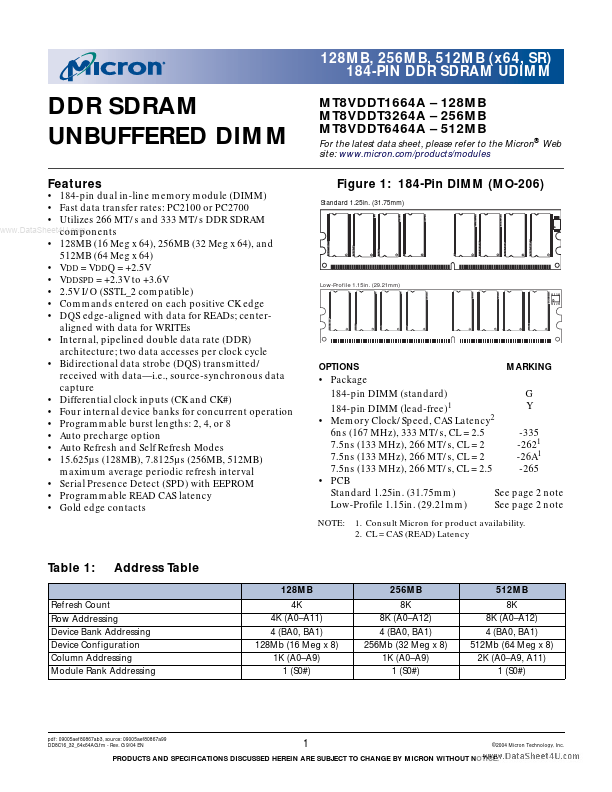
- 184-pin dual in-line memory module (DIMM)
- Fast data transfer rates: PC2100 or PC2700
- VDD = VDDQ = +2.5V
- VDDSPD = +2.3V to +3.6V
- mands entered on each positive CK edge
- DQS edge-aligned with data for READs; centeraligned with data for WRITEs
- Internal, pipelined double data rate (DDR) architecture; two data accesses per clock cycle
- Bidirectional data strobe (DQS) transmitted/ received with data—i.e., source-synchronous data capture
- Differential clock inputs (CK and CK#)
- Four internal device banks for concurrent operation