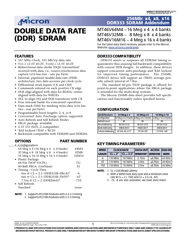
46V16M16 Overview
Key Features
- 167 MHz Clock, 333 Mb/s/p data rate
- VDD = +2.5V ±0.2V, VDDQ = +2.5V ±0.2V
- Bidirectional data strobe (DQS) transmitted/ received with data, i.e., source-synchronous data capture (x16 has two
- one per byte)
- Internal, pipelined double-data-rate (DDR) architecture; two data accesses per clock cycle
- Differential clock inputs (CK and CK#)
- Commands entered on each positive CK edge
- DQS edge-aligned with data for READs; centeraligned with data for WRITEs
- DLL to align DQ and DQS transitions with CK
- Four internal banks for concurrent operation