MT16LSDT6464A
MT16LSDT6464A is SYNCHRONOUS DRAM MODULE manufactured by Micron Technology.
..
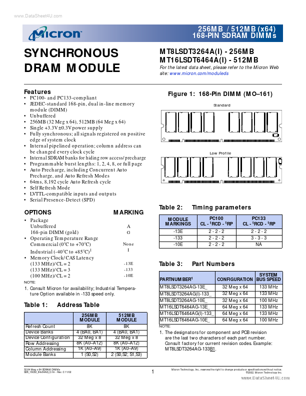
256MB / 512MB (x64) 168-PIN SDRAM DIMMs
SYNCHRONOUS DRAM MODULE
Features
- PC100- and PC133-pliant
- JEDEC-standard 168-pin, dual in-line memory module (DIMM)
- Unbuffered
- 256MB (32 Meg x 64), 512MB (64 Meg x 64)
- Single +3.3V ±0.3V power supply
- Fully synchronous; all signals registered on positive edge of system clock
- Internal pipelined operation; column address can be changed every clock cycle
- Internal SDRAM banks for hiding row access/precharge
- Programmable burst lengths: 1, 2, 4, 8, or full page
- Auto Precharge, including Concurrent Auto Precharge, and Auto Refresh Modes
- 64ms, 8,192 cycle Auto Refresh cycle
- Self Refresh Mode
- LVTTL-patible...