Datasheet4U.com
🌙
MT28F200B5 Datasheet | Micron Technology
Part:
MT28F200B5
Description:
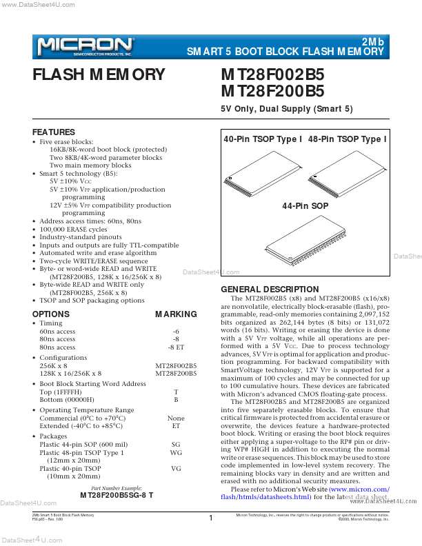
FLASH MEMORY
Manufacturer:
Micron Technology
Size:
833.63 KB
MT28F200B5 Datasheet (PDF) Download
Related MT28F200B5 Datasheets
MT28F200B3 FLASH MEMORY
Micron Technology
MT28F200B5
Key Features
1 Micron Technology, Inc., reserves the right to change products or specifications without notice
©2000, Micron Technology, Inc
×
Close