MT46V128M8
Description
The 1Gb DDR SDRAM is a high-speed CMOS, dynamic random-access memory containing 1,073,741,824 bits.
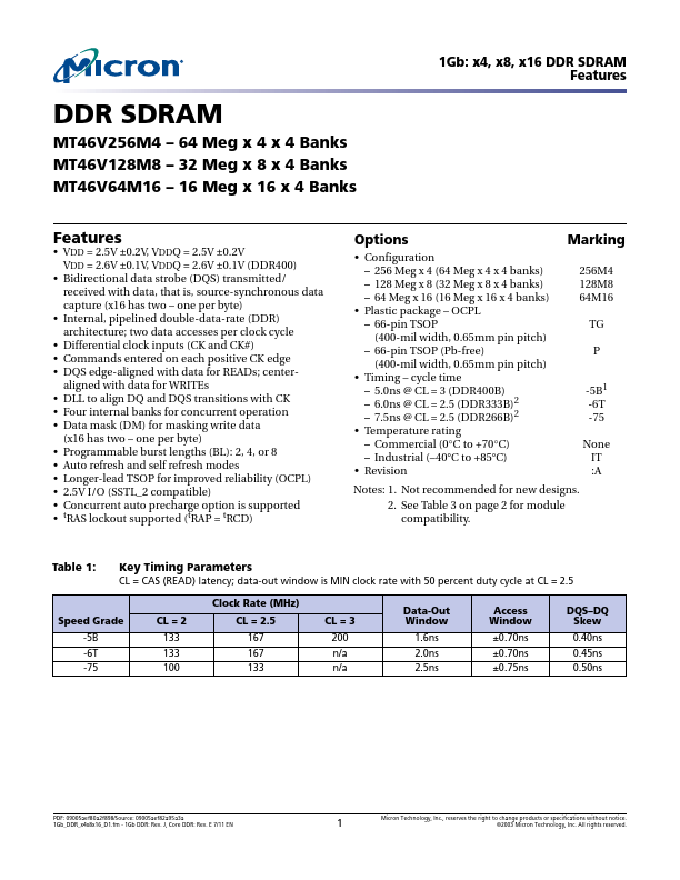
Key Features
- Bidirectional data strobe (DQS) transmitted/ received with data, i.e., source-synchronous data capture (x16 has two – one per byte)
- Internal, pipelined double-data-rate (DDR) architecture; two data accesses per clock cycle
- Differential clock inputs (CK and CK#)
- mands entered on each positive CK edge
- DQS edge-aligned with data for READs; centeraligned with data for WRITEs
- DLL to align DQ and DQS transitions with CK
- Four internal banks for concurrent operation
- Data mask (DM) for masking write data (x16 has two –one per byte)
- Auto Refresh and Self Refresh Modes
- Longer lead TSOP for improved reliability (OCPL)