Datasheet Summary
1 MEG x 16 FPM DRAM
FPM DRAM
Features
- JEDEC- and industry-standard x16 timing, functions, pinouts, and packages
- High-performance, low-power CMOS silicon-gate process
- Single power supply (+3.3V ±0.3V or 5V ±0.5V)
- All inputs, outputs and clocks are TTL-patible
- Refresh modes: RAS#-ONLY, CAS#-BEFORE-RAS# (CBR) and HIDDEN
- Optional self refresh (S) for low-power data retention
- BYTE WRITE and BYTE READ access cycles
- 1,024-cycle refresh (10 row, 10 column addresses)
- FAST-PAGE-MODE (FPM) access
MT4C1M16C3, MT4LC1M16C3
For the latest data sheet revisions, please refer to the Micron Web site: .micron./datasheets
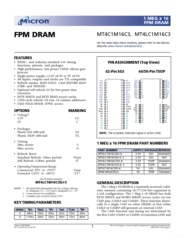
PIN ASSIGNMENT (Top View) 42-Pin SOJ
VCC DQ0 DQ1 DQ2 DQ3...