EDI88512CA Overview
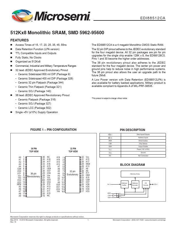
Data Inputs/Outputs Address Inputs Write Enables Chip Selects Output Enable Power (+5V ±10%) Ground Not Connected BLOCK DIAGRAM Memory Array A0-18 WE# CS# OE# Address Buffer Address Decoder I/O Circuits I/O0-7 Microsemi Corporation reserves the right to change products or specifications without notice. May 2014 © 2014 Microsemi Corporation. Stress greater than those listed.
EDI88512CA Key Features
- Ceramic Sidebrazed 600 mil DIP (Package 9)
- Ceramic Sidebrazed 400 mil DIP (Package 326)
- Ceramic 32 pin Flatpack (Package 344)
- Ceramic Thin Flatpack (Package 321)
- Ceramic SOJ (Package 140) - 36 lead JEDEC Approved Revolutionary Pinout
- Ceramic Flatpack (Package 316)
- Ceramic SOJ (Package 327)
- Ceramic LCC (Package 502) - Single +5V (±10%) Supply Operation
EDI88512CA Applications
- This product is subject to change without notice