SG1527A
Description
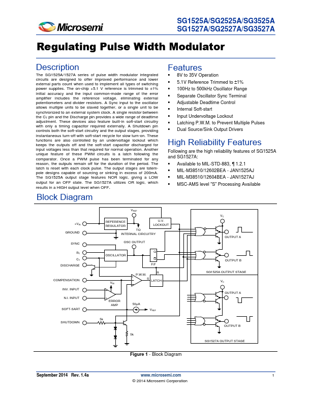
The SG1525A/1527A series of pulse width modulator integrated circuits are designed to offer improved performance and lower external parts count when used to implement all types of switching power supplies. The on-chip +5.1 V reference is trimmed to ±1% initial accuracy and the input common-mode range of the error amplifier includes the reference voltage, eliminating external potentiometers and divider resistors.