Datasheet4U.com
🌙
ZL40260 Datasheet | Microsemi
Part:
ZL40260
Description:
Low Additive Jitter 2 x10 LVPECL Fanout Buffer
Manufacturer:
Microsemi
Size:
776.02 KB
Download ZL40260 Datasheet PDF
Microsemi
ZL40260
Key Features
Two inputs accept any differential (LVPECL, HCSL, LVDS, SSTL, CML) or single ended LVCMOS signal
Applications
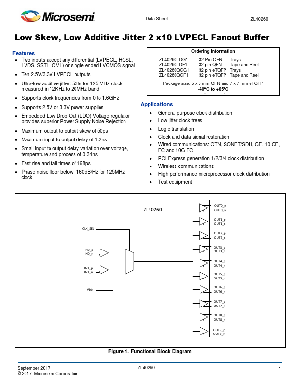
Functional ZL40260
×
Close