MT8985 Overview
Key Specifications
Package: DIP
Operating Voltage: 5 V
Length: 51.75 mm
Width: 15.24 mm
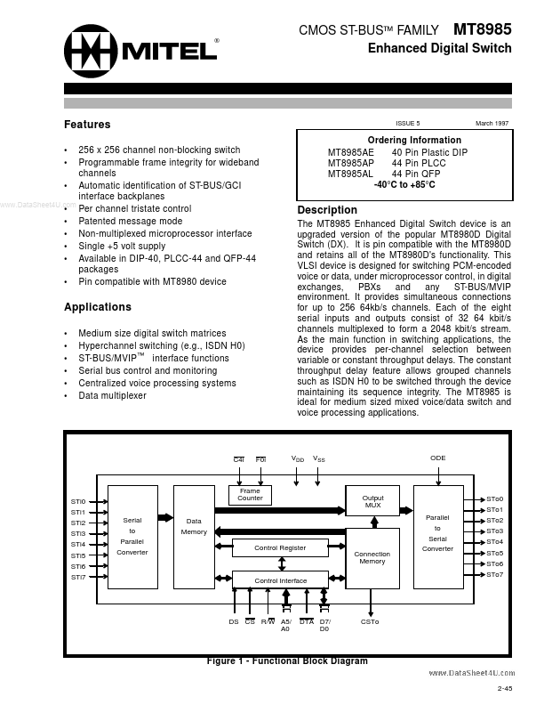
Description
The MT8985 Enhanced Digital Switch device is an upgraded version of the popular MT8980D Digital Switch (DX). It is pin compatible with the MT8980D and retains all of the MT8980D's functionality.
Key Features
- Automatic identification of ST-BUS/GCI interface backplanes
- Per channel tristate control
- Patented message mode
- Non-multiplexed microprocessor interface
- Single +5 volt supply