SL6140
SL6140 is 400MHz Wideband AGC Amplifier manufactured by Mitel Networks Corporation.
400MHz Wideband AGC Amplifier
DS2159 Issue no 5.0 July 1999
Features
Ordering Information
G G G G G G
400MHz Bandwidth (RL=50Ω) High voltage Gain 45d B (RL=1kΩ) 70d B Gain Control Range High Output Level at Low Gain Surface Mount Plastic Package Low Cost
SL6140/NA/MP
Industrial temperature range miniature plastic package SL6140/NA/MPTC Tape and Reel
Applications
RF/IF Amplifier High Gain Mixers Video Amplifiers
Description
The SL6140 is an integrated broadband AGC amplifier, designed on an advanced bipolar process. The amplifier provides over 15d B of linear gain into 50Ω at 400MHz. Gain control is also provided with over 70d B of dynamic range. The SL6140 offers over 45d B of voltage gain with an RL of 1kΩ.
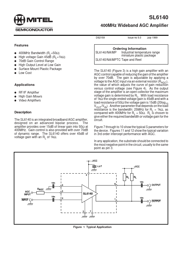
The SL6140 (Figure 3) is a high gain amplifier with an AGC control capable of reducing the gain of the amplifier by over 70d B. The gain is adjustable by applying a voltage to the AGC input via an external resistor (RAGC), the value of which adjusts the curve of gain reduction versus control voltage (see Figure 4). As the output stage of the amplifier is an open collector the maximum voltage gain is determined by RL. With load resistance of 1kΩ the single ended voltage gain is 45d B and with a load resistance of 50Ω the voltage gain is 15d B (20log10 VOUT/VIN). Another parameter that depends on the load resistance is the bandwidth: 25MHz for RL = 1kΩ, as pared with 400MHz for RL = 50Ω. RL is chosen to give either the required bandwidth or voltage gain for the circuit. Figure 7 through to 10 show the typical S parameters for the device. Figures 11 and 12 show the typical variation in 3rd order intercept performance with AGC. In any application, the substrate should be connected to the most negative point in the circuit, usually to the same point as pin 3.
+VCC 1.0 F +VCC
2 RL 10n RAGC AGC INPUT 10n INPUT 6 5 8 RL 10n OUTPUT
4 1 10n OUTPUT
Figure 1 Typical Application
OUTPUT +VCC GROUND INPUT
1 2 3 4
8 7 6...