M2S28D30ATP-10 Key Features
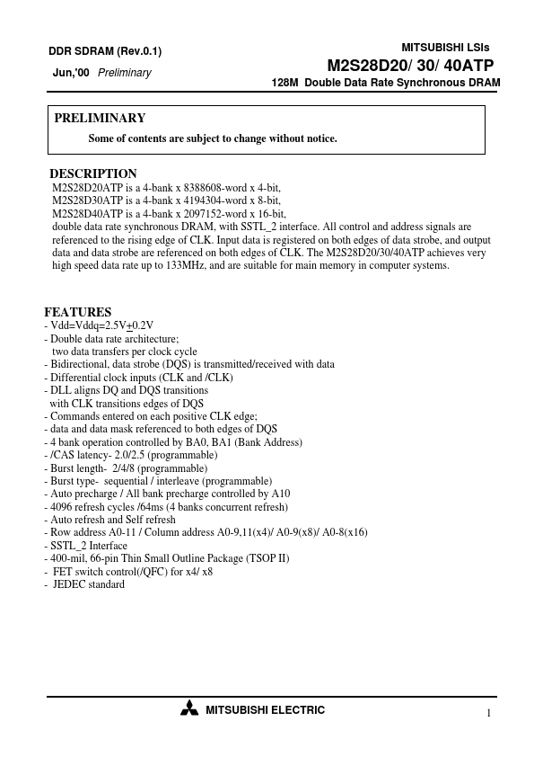
- Vdd=Vddq=2.5V+0.2V
- Double data rate architecture; two data transfers per clock cycle
- Bidirectional, data strobe (DQS) is transmitted/received with data
- Differential clock inputs (CLK and /CLK)
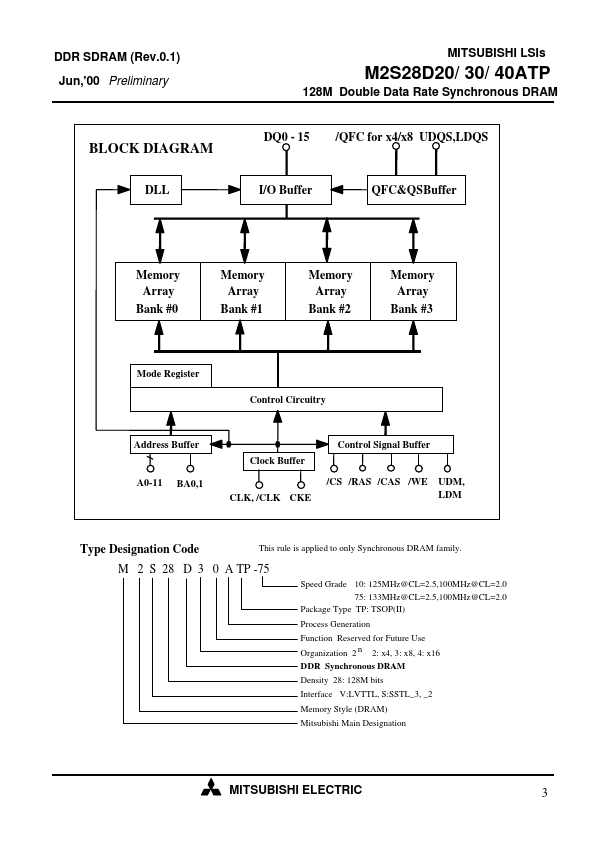
- DLL aligns DQ and DQS transitions with CLK transitions edges of DQS
- mands entered on each positive CLK edge
- data and data mask referenced to both edges of DQS
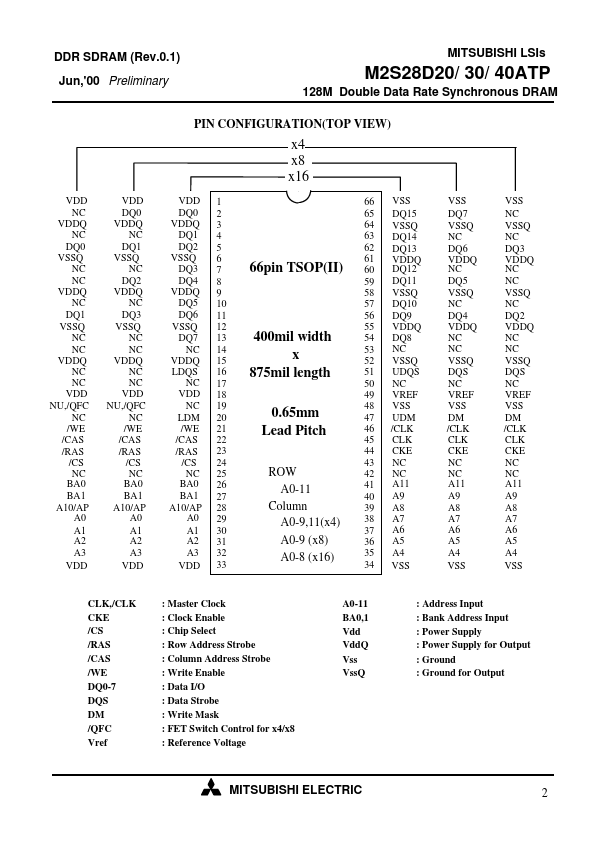
- 4 bank operation controlled by BA0, BA1 (Bank Address)
- /CAS latency- 2.0/2.5 (programmable)
- Burst length- 2/4/8 (programmable)


